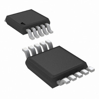
LM5067MM-2/NOPB National Semiconductor, LM5067MM-2/NOPB Datasheet - Page 20

LM5067MM-2/NOPB
Manufacturer Part Number
LM5067MM-2/NOPB
Description
IC CTLR NEG HOTSWAP A/R 10MSOP
Manufacturer
National Semiconductor
Type
Hot-Swap Controllerr
Datasheet
1.LM5067MM-1NOPB.pdf
(24 pages)
Specifications of LM5067MM-2/NOPB
Applications
General Purpose
Internal Switch(s)
No
Voltage - Supply
-9 V ~ -80 V
Operating Temperature
-40°C ~ 125°C
Mounting Type
Surface Mount
Package / Case
10-TFSOP, 10-MSOP (0.118", 3.00mm Width)
For Use With
LM5067EVAL - NEGATIVE HOT SWAP / INRUSH CURRE
Lead Free Status / RoHS Status
Lead free / RoHS Compliant
Other names
LM5067MM-2TR
Available stocks
Company
Part Number
Manufacturer
Quantity
Price
Company:
Part Number:
LM5067MM-2/NOPB
Manufacturer:
TI
Quantity:
4 500
www.national.com
POWER GOOD PIN
During initial power up, the Power Good pin (PGD) is high until
the operating voltage (VCC – VEE) increases above
PGD then switches low, remaining low as the system voltage
and the operating voltage increase. After Q1 is switched on,
when the voltage at the OUT pin is within 1.23V of the SENSE
pin (Q1’s V
put voltage is at, or nearly at, its final value. Any of the
following situations will cause PGD to switch low within
µs:
- The V
- The system input voltage decreases below the UVLO level.
- The system input voltage increase above the OVLO level.
- The TIMER pin increases to 4V due to a fault condition.
A pull-up resistor is required at PGD as shown in Figure 15.
The pull-up voltage (V
with transient capability to 100V, and can be higher or lower
than the system ground.
Design-in Procedure
The recommended design-in procedure for the LM5067 is as
follows:
•
•
•
Determine the minimum and maximum system voltages
(VEE). Select the input resistor (R
mA into the VCC pin at the minimum system voltage.The
resistor’s power rating must be suitable for its power
dissipation at maximum system voltage ((V
R
Determine the current limit threshold (I
must be higher than the normal maximum load current,
allowing for tolerances in the current sense resistor value
and the LM5067 Current Limit threshold voltage. Use
equation 1 to determine the value for R
Determine the maximum allowable power dissipation for
the series pass FET (Q1), using the device’s SOA
information. Use equation 2 to determine the value for
R
IN
PWR
).
DS
.
of Q1 increases above 2.5V.
DS
<1.23V), PGD switches high indicating the out-
PGD
) can be as high as 80V above VEE,
FIGURE 16. Adding Delay to the Power Good Output Pin
IN
) to provide at least 2
LIM
S
.
). This threshold
SYS
– 13V)
≊
≊
2V.
2
10
/
20
If a delay is required at PGD, suggested circuits are shown in
Figure 16. In Figure 16a, capacitor C
ing edge, but not to the falling edge. In Figure 16b, the rising
edge is delayed by R
edge is delayed a lesser amount by R
diode across R
two edges, or a short delay at the rising edge and a long delay
at the falling edge.
•
•
•
Determine the value for the timing capacitor at the TIMER
pin (C
(t
time. The turn-on time can be estimated using the
equations in the Turn-on Time section of this data sheet,
but should be verified experimentally. Allow for tolerances
in the values of the external capacitors, sense resistor, and
the LM5067 Electrical Characteristics for the TIMER pin,
current limit and power limt. Review the resulting insertion
time, and the restart timing if the LM5067-2 is used.
Choose option A, B, C, or D from the UVLO, OVLO section
of the Application Information for setting the UVLO and
OVLO thresholds and hysteresis. Use the procedure in the
appropriate option to determine the resistor values at the
UVLO and OVLO pins.
Choose the appropriate voltage, and pull-up resistor, for
the Power Good output.
FAULT
T
) must be longer than the circuit’s turn-on-
) using equation 3. The fault timeout period
FIGURE 15. Power Good Output
PG2
(Figure 16c) allows for equal delays at the
PG1
+ R
PG2
and C
PG
PG2
adds delay to the ris-
PG
and C
, while the falling
30030958
PG
30030959
. Adding a


