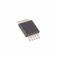
MAX5924DEUB+T Maxim Integrated Products, MAX5924DEUB+T Datasheet - Page 2

MAX5924DEUB+T
Manufacturer Part Number
MAX5924DEUB+T
Description
IC HOT-SWAP CTRLR N-CH 10-UMAX
Manufacturer
Maxim Integrated Products
Type
Hot-Swap Controllerr
Datasheet
1.MAX5925AEUB.pdf
(21 pages)
Specifications of MAX5924DEUB+T
Applications
General Purpose
Internal Switch(s)
No
Voltage - Supply
1 V ~ 13.2 V
Operating Temperature
-40°C ~ 85°C
Mounting Type
Surface Mount
Package / Case
10-MSOP, Micro10™, 10-uMAX, 10-uSOP
Lead Free Status / RoHS Status
Lead free / RoHS Compliant
ABSOLUTE MAXIMUM RATINGS
(All voltages referenced to GND, unless otherwise noted.)
V
GATE*.....................................................................-0.3V to +20V
All Other Pins ............-0.3V to the lower of (V
SC_DET Current (200ms pulse width, 15% duty cycle) ...140mA
Continuous Current (all other pins) .....................................20mA
1V to 13.2V, n-Channel Hot-Swap Controllers
Require No Sense Resistor
* GATE is internally driven and clamped. Do not drive GATE with external source.
Stresses beyond those listed under “Absolute Maximum Ratings” may cause permanent damage to the device. These are stress ratings only, and functional
operation of the device at these or any other conditions beyond those indicated in the operational sections of the specifications is not implied. Exposure to
absolute maximum rating conditions for extended periods may affect device reliability.
ELECTRICAL CHARACTERISTICS
(V
T
open, T
2
POWER SUPPLIES
V
V
Supply Current
UNDERVOLTAGE LOCKOUT (UVLO)
UVLO Threshold
V
V
LOAD-PROBE
Load-Probe Resistance (Note 3)
Load-Probe Timeout
Load-Probe Threshold Voltage
CIRCUIT BREAKER
Circuit-Breaker Programming
Current
CC
A
CC
CC
S
CC
CC
= -40°C to +85°C, unless otherwise noted. Typical values are at V
Operating Range
_______________________________________________________________________________________
.........................................................................-0.3V to +14V
, EN (MAX5924/MAX5925), EN1 (MAX5926) = +2.7V to +13.2V; EN2 (MAX5926) = 0V; V
Operating Range
UVLO Deglitch Time
UVLO Startup Delay
A
= +25°C, unless otherwise noted.) (Note 1)
PARAMETER
SYMBOL
t
V
D,UVLO
V
I
I
V
CB25
CB85
LP,TH
UVLO
t
R
I
I
t
V
DG
CC
CB
CC
LP
LP
S
CC
+ 0.3V) or +14V
V
FET is fully enhanced, SC_DET = V
D efaul t val ue, V
(Note 2)
2.7V < V
5V < V
(Note 4)
TC = high
(MAX5926), MAX5924
TC = low (MAX5926),
MAX5925 (Note 5)
TC = low (MAX5926),
MAX5925 (Note 5)
S
as defined in Figure 1
CC
CC
< 13.2V
< 5V
S
CONDITIONS
and V
Continuous Power Dissipation (T
Operating Temperature Range ...........................-40°C to +85°C
Junction Temperature .....................................................+150°C
Storage Temperature Range .............................-65°C to +150°C
Lead Temperature (soldering, 10s) .................................+300°C
Soldering Temperature (reflow) .......................................+260°C
CC
C C
10-Pin µMAX (derate 6.9mW/°C above +70°C) ...........556mW
16-Pin QSOP (derate 18.9mW/°C above +70°C).......1509mW
V
= 1V
2.7V ≤ V
V
1V, T
2.7V ≤ V
T
V
= 1V, T
2.7V ≤ V
T
i ncr easi ng , Fi g ur e 1
= 5V, R L = 500Ω from OUT to GND, C L = 1µF, SLEW =
A
A
CC
CC
CC
= +25°C
= +85°C
= 2.7V and V
= 2.7V, V
= 2.7V and V
A
= +25°C
A
CC
CC
CC
= +85°C
CC
≤ 13.2V
≤ 13.2V,
≤ 13.2V,
CB
=
CB
CB
S
MIN
1.73
123
172
2.7
1.0
43
34
30
40
40
50
(see Figure 1) = +1.05V to V
4
3
A
= +70°C)
TYP
2.06
900
200
102
200
1.5
30
10
37
37
40
50
50
60
MAX
13.2
2.47
V
350
205
235
2.5
65
20
42
50
60
60
70
CC
UNITS
mA
mV
ms
ms
µA
µs
Ω
V
V
V
CC
;


