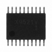
X9521V20I Intersil, X9521V20I Datasheet - Page 13

X9521V20I
Manufacturer Part Number
X9521V20I
Description
IC LASR CTRLR 2CHAN 5.5V 20TSSOP
Manufacturer
Intersil
Type
Laser Diode Controller (Fiber Optic)r
Datasheet
1.X9521V20I.pdf
(24 pages)
Specifications of X9521V20I
Number Of Channels
2
Voltage - Supply
2.7 V ~ 5.5 V
Current - Supply
1.5mA
Operating Temperature
-40°C ~ 85°C
Package / Case
20-TSSOP
Mounting Type
Surface Mount
Lead Free Status / RoHS Status
Contains lead / RoHS non-compliant
Other names
X9521V20I-A
X9521V20I-A
X9521V20I-A
The region of EEPROM memory which is protected /
locked is determined by the combination of the BL1 and
BL0 bits written to the CONSTAT register. It is possible to
lock the regions of EEPROM memory shown in the table
below:
If the user attempts to perform a write operation on a pro-
tected region of EEPROM memory, the operation is
aborted without changing any data in the array.
When the Block Lock bits of the CONSTAT register are
set to something other than BL1 = 0 and BL0 = 0, then
the “wiper position” of the DCPs cannot be changed - i.e.
DCP write operations cannot be conducted:
The factory default setting for these bits are BL1 = 0,
BL0 = 0.
IMPORTANT NOTE: If the Write Protect (WP) pin of the
X9521 is active (HIGH), then all nonvolatile write opera-
tions to both the EEPROM memory and DCPs are inhib-
ited, irrespective of the Block Lock bit settings (See "WP:
Write Protection Pin").
CONSTAT Register Write Operation
The CONSTAT register is accessed using the Slave
Address set to 1010010 (Refer to Figure 4.). Following
the Slave Address Byte, access to the CONSTAT regis-
ter requires an Address Byte which must be set to FFh.
BL1 BL0
SCL
SDA
BL1
0
0
1
1
0
0
1
1
0
1
0
1
S
T
A
R
T
BL0
0
1
0
1
1
Protected Addresses
80h - FFh
00h - FFh
C0h - FFh
SLAVE ADDRESS BYTE
0
None (Default)
DCP Write Operation Permissible
1
(Size)
0
(128 bytes
(256 bytes)
(64 bytes
Figure 18. CONSTAT Register Write Command Sequence
0
13
YES (Default)
1
)
)
NO
NO
NO
0
R/W A
Partition of array
None (Default)
C
K
Upper 1/4
Upper 1/2
locked
1
All
1
ADDRESS BYTE
1
X9521
1
1
1
Only one data byte is allowed to be written for each
CONSTAT register Write operation. The user must issue
a STOP, after sending this byte to the register, to initiate
the nonvolatile cycle that stores the BP1and BP0 bits.
The X9521 will not ACKNOWLEDGE any data bytes
written after the first byte is entered (Refer to Figure 18.).
When writing to the CONSTAT register, the bits CS7-
CS5 and CS0 must all be set to “0”. Writing any other bit
sequence to bits CS7-CS5 and CS0 of the CONSTAT
register is reserved.
Prior to writing to the CONSTAT register, the WEL and
RWEL bits must be set using a two step process, with
the whole sequence requiring 3 steps
—Write a 02H to the CONSTAT Register to set the Write
—Write a 06H to the CONSTAT Register to set the Reg-
—Write a one byte value to the CONSTAT Register that
Enable Latch (WEL). This is a volatile operation, so
there is no delay after the write. (Operation preceded
by a START and ended with a STOP).
ister Write Enable Latch (RWEL) AND the WEL bit.
This is also a volatile cycle. The zeros in the data byte
are required. (Operation preceded by a START and
ended with a STOP).
has all the bits set to the desired state. The CONSTAT
register can be represented as 000st010 in binary,
where st are the Block Lock Protection (BL1 and BL0)
bits. This operation is proceeded by a START and
ended with a STOP bit. Since this is a nonvolatile write
cycle, it will typically take 5ms to complete. The RWEL
bit is reset by this cycle and the sequence must be
repeated to change the nonvolatile bits again. If bit 2 is
set to ‘1’ in this third step (000s t110) then the RWEL
bit is set, but the BL1 and BL0 bits remain unchanged.
Writing a second byte to the control register is not
allowed. Doing so aborts the write operation and the
X9521 does not return an ACKNOWLEDGE.
1
1
A
C
K
CS7 CS6 CS5 CS4 CS3 CS2 CS1 CS0
CONSTAT REGISTER DATA IN
September 21, 2010
A
C
K
S
T
O
P
FN8207.2


