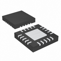
MAX3735AETG+ Maxim Integrated Products, MAX3735AETG+ Datasheet - Page 9

MAX3735AETG+
Manufacturer Part Number
MAX3735AETG+
Description
IC LSR DRVR 2.7GBPS 3.63V 24TQFN
Manufacturer
Maxim Integrated Products
Type
Laser Diode Driver (Fiber Optic)r
Datasheet
1.MAX3735AETGT.pdf
(18 pages)
Specifications of MAX3735AETG+
Data Rate
2.7Gbps
Number Of Channels
1
Voltage - Supply
2.97 V ~ 3.63 V
Current - Supply
27mA
Current - Modulation
85mA
Current - Bias
100mA
Operating Temperature
-40°C ~ 85°C
Package / Case
24-TQFN Exposed Pad
Mounting Type
Surface Mount
Operating Supply Voltage
3.3 V
Supply Current
27 mA
Maximum Operating Temperature
+ 85 C
Maximum Power Dissipation
1354 mW
Minimum Operating Temperature
- 40 C
Mounting Style
SMD/SMT
Lead Free Status / RoHS Status
Lead free / RoHS Compliant
The MAX3735/MAX3735A laser drivers consist of three
parts: a high-speed modulation driver, a laser-biasing
block with automatic power control (APC), and safety
circuitry (Figure 4). The circuit design is optimized for
high-speed and low-voltage (+3.3V) operation.
The output stage are composed of a high-speed differ-
ential pair and a programmable modulation current
source. The MAX3735/MAX3735A are optimized for dri-
ving a 15Ω load; the minimum instantaneous voltage
required at OUT+ is 0.6V. Modulation current swings up
to 60mA are possible when the laser diode is DC-cou-
pled to the driver and up to 85mA when the laser diode
is AC-coupled to the driver.
1, 4, 8, 14, 18
7, 12, 22
15, 16
PIN
EP
10
11
13
17
19
20
21
23
24
2
3
5
6
9
SHUTDOWN
TX_DISABLE
TX_FAULT
APCFILT1
APCFILT2
BC_MON
PC_MON
MODSET
Exposed
APCSET
NAME
High-Speed Modulation Driver
OUT+
OUT-
GND
BIAS
V
IN+
Pad
MD
_______________________________________________________________________________________
IN-
CC
2.7Gbps, Low-Power SFP Laser Drivers
Detailed Description
+3.3V Supply Voltage
Noninverted Data Input
Inverted Data Input
Photodiode Current Monitor Output. Current out of this pin develops a ground-referenced voltage
across an external resistor that is proportional to the monitor diode current.
Bias Current Monitor Output. Current out of this pin develops a ground-referenced voltage across an
external resistor that is proportional to the bias current.
Ground
Shutdown Driver Output. Voltage output to control an external transistor for optional shutdown
circuitry.
Open-Collector Transmit Fault Indicator (Table 1).
A resistor connected from this pad to ground sets the desired modulation current.
Laser Bias Current Output
Noninverted Modulation Current Output. Connect pins 15 and 16 externally to minimize parasitic
inductance of the package. I
Inverted Modulation Current Output. I
Monitor Diode Input. Connect this pin to the anode of a monitor photodiode. A capacitor to ground is
required to filter the high-speed AC monitor photocurrent.
Connect a capacitor (C
pole of the APC feedback loop.
See APCFILT1
A resistor connected from this pin to ground sets the desired average optical power.
Transmitter Disable, TTL. Laser output is disabled when TX_DISABLE is asserted high or left
unconnected. The laser output is enabled when this pin is asserted low.
Ground. Must be soldered to the circuit board ground for proper thermal and electrical performance
(see the Exposed Pad Package section).
APC
) between pin 20 (APCFILT1) and pin 21 (APCFILT2) to set the dominant
MOD
flows into this pin when input data is high.
MOD
To interface with the laser diode, a damping resistor
(R
bined resistance of the series damping resistor and the
equivalent series resistance of the laser diode should
equal 15Ω. To reduce optical output aberrations and
duty-cycle distortion caused by laser diode parasitic
inductance, an RC shunt network might be necessary.
Refer to Maxim Application Note HFAN 02.0: Interfacing
Maxim’s Laser Drivers to Laser Diodes for more informa-
tion.
At data rates of 2.7Gbps, any capacitive load at the
cathode of a laser diode degrades optical output perfor-
mance. Because the BIAS output is directly connected
to the laser cathode, minimize the parasitic capacitance
associated with the pin by using an inductor to isolate
the BIAS pin parasitics from the laser cathode.
D
flows into this pin when input data is low.
) is required for impedance matching. The com-
FUNCTION
Pin Description
9


