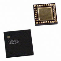
TZA3011BVH/C2,551 NXP Semiconductors, TZA3011BVH/C2,551 Datasheet - Page 8

TZA3011BVH/C2,551
Manufacturer Part Number
TZA3011BVH/C2,551
Description
IC LASER DRIVER 3.2GBPS 32-HBCC
Manufacturer
NXP Semiconductors
Series
A-rate™r
Type
Laser Diode Driver (Fiber Optic)r
Datasheet
1.TZA3011AVHC2557.pdf
(30 pages)
Specifications of TZA3011BVH/C2,551
Data Rate
3.2Gbps
Number Of Channels
1
Voltage - Supply
3.14 V ~ 3.47 V
Current - Supply
40mA
Current - Modulation
100mA
Current - Bias
100mA
Operating Temperature
-40°C ~ 85°C
Package / Case
32-HBCC
Mounting Type
Surface Mount
Lead Free Status / RoHS Status
Lead free / RoHS Compliant
Other names
935269941551
TZA3011BVHW-S
TZA3011BVHW-S
TZA3011BVHW-S
TZA3011BVHW-S
Philips Semiconductors
7. Functional description
9397 750 14437
Product data sheet
7.1 Data and clock input
Table 3:
[1]
[2]
[3]
Table 4:
The TZA3011 operates with differential Positive Emitter Coupled Logic (PECL), Low
Voltage Positive Emitter Coupled Logic (LVPECL) and Current-Mode Logic (CML) data
and clock inputs with a voltage swing from 100 mV to 1 V (p-p). It is assumed that both the
data and clock inputs carry a complementary signal with the specified peak-to-peak value
(true differential excitation).
Symbol
GNDESD
MON
BIASIN
BIASOUT
GNDCCB
MODIN
GNDCCB
i.c.
MODOUT
ER
AVR
Parameter
Glass passivation
Bonding pad dimension
Metallization
Thickness
Size
Backing
Attach temperature
Attach time
All GND connections should be used.
All ground pads must be connected to ground.
Recommended order of bonding: all GND first, then V
output pins.
All coordinates are referenced, in m, to the center of the die.
Pad is internally connected, do not use.
ACDC pad must be left unconnected for AC-coupling applications. For DC-coupling applications, connect
this pad to ground.
Bonding pad description TZA3011UH
Physical characteristics of TZA3011UH
Pad
47
48
49
50
51
52
53
54
55
56
57
[2]
Rev. 06 — 20 January 2005
X
765.0
602.1
431.7
267.6
100.8
Value
0.3 m PSG (Phospho Silicate Glass) on top of 0.8 m of silicon nitride
minimum dimension of exposed metallization is 80 m
size = 90 m
2.8 m AlCu
380 m nominal
2.560 mm
silicon; electrically connected to GND potential through substrate
contacts
< 440 C; recommended die attachment is by gluing
< 15 s
82.7
241.1
274.4
487.2
645.6
802.8
Y
1123.8
1123.7
1123.8
1123.8
1123.8
+1123.8
+1123.8
+954.4
+1123.8
+1123.8
+1123.8
2.510 mm (6.43 mm
90 m)
30 Mbit/s up to 3.2 Gbit/s A-rate
TZA3011A; TZA3011B
Description
ground
input for the monitor photodiode (RF input)
input for the bias current setting
output of the control block for the bias current
ground
input for the modulation current setting
ground
internally connected
output of the control block for the modulation
current
input for the optical extinction ratio setting
input for the optical average power level setting
CCA
[1]
…continued
,V
CCD
2
)
and V
© Koninklijke Philips Electronics N.V. 2005. All rights reserved.
CCO
supplies and finally the input and
80 m (pad
laser drivers
8 of 30


