LP5521TMX/NOPB National Semiconductor, LP5521TMX/NOPB Datasheet - Page 24
LP5521TMX/NOPB
Manufacturer Part Number
LP5521TMX/NOPB
Description
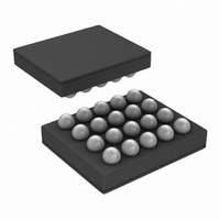
IC LED DRIVER RGB 25-USMD
Manufacturer
National Semiconductor
Series
PowerWise®r
Type
RGB LED Driverr
Datasheet
1.LP5521TMNOPB.pdf
(40 pages)
Specifications of LP5521TMX/NOPB
Constant Current
Yes
Topology
PWM, Switched Capacitor (Charge Pump)
Number Of Outputs
3
Internal Driver
Yes
Type - Primary
Backlight, Light Management Unit (LMU)
Type - Secondary
RGB
Frequency
1.25MHz
Voltage - Supply
2.7 V ~ 5.5 V
Voltage - Output
4.55V
Mounting Type
Surface Mount
Package / Case
20-MicroSMD
Operating Temperature
-30°C ~ 85°C
Current - Output / Channel
25.5mA
Internal Switch(s)
Yes
Efficiency
95%
Lead Free Status / RoHS Status
Lead free / RoHS Compliant
Other names
LP5521TMX
Available stocks
Company
Part Number
Manufacturer
Quantity
Price
Company:

Part Number:
LP5521TMX/NOPB
Manufacturer:
TI
Quantity:
57 001
Part Number:
LP5521TMX/NOPB
Manufacturer:
TI/德州仪器
Quantity:
20 000


www.national.com
I
Interface Bus Overview
The I
cess to the programmable functions and registers on the
device. This protocol uses a two-wire interface for bidirec-
tional communications between the IC's connected to the bus.
The two interface lines are the Serial Data Line (SDA), and
the Serial Clock Line (SCL). These lines should be connected
to a positive supply, via a pull-up resistor and remain HIGH
even when the bus is idle.
Every device on the bus is assigned a unique address and
acts as either a Master or a Slave depending on whether it
generates or receives the serial clock (SCL).
Data Transactions
One data bit is transferred during each clock pulse. Data is
sampled during the high state of the serial clock (SCL). Con-
sequently, throughout the clock’s high period, the data should
remain stable. Any changes on the SDA line during the high
state of the SCL and in the middle of a transaction, aborts the
current transaction. New data should be sent during the low
SCL state. This protocol permits a single data line to transfer
both command/control information and data using the syn-
chronous serial clock.
Each data transaction is composed of a Start Condition, a
number of byte transfers (set by the software) and a Stop
Condition to terminate the transaction. Every byte written to
the SDA bus must be 8 bits long and is transferred with the
most significant bit first. After each byte, an Acknowledge sig-
nal must follow. The following sections provide further details
of this process.
2
C Compatible Serial Bus Interface
2
C compatible synchronous serial interface provides ac-
Acknowledge Signal
Data Validity
20186249
20186220
24
The Master device on the bus always generates the Start and
Stop Conditions (control codes). After a Start Condition is
generated, the bus is considered busy and it retains this sta-
tus until a certain time after a Stop Condition is generated. A
high-to-low transition of the data line (SDA) while the clock
(SCL) is high indicates a Start Condition. A low-to-high tran-
sition of the SDA line while the SCL is high indicates a Stop
Condition.
In addition to the first Start Condition, a repeated Start Con-
dition can be generated in the middle of a transaction. This
allows another device to be accessed, or a register read cycle.
Acknowledge Cycle
The Acknowledge Cycle consists of two signals: the acknowl-
edge clock pulse the master sends with each byte transferred,
and the acknowledge signal sent by the receiving device.
The master generates the acknowledge clock pulse on the
ninth clock pulse of the byte transfer. The transmitter releases
the SDA line (permits it to go high) to allow the receiver to
send the acknowledge signal. The receiver must pull down
the SDA line during the acknowledge clock pulse and ensure
that SDA remains low during the high period of the clock
pulse, thus signaling the correct reception of the last data byte
and its readiness to receive the next byte.
“ACKNOWLEDGE AFTER EVERY BYTE” RULE
The master generates an acknowledge clock pulse after each
byte transfer. The receiver sends an acknowledge signal after
every byte received.
There is one exception to the “acknowledge after every byte”
rule. When the master is the receiver, it must indicate to the
transmitter an end of data by not-acknowledging (“negative
acknowledge”) the last byte clocked out of the slave. This
“negative acknowledge” still includes the acknowledge clock
pulse (generated by the master), but the SDA line is not pulled
down.
ADDRESSING TRANSFER FORMATS
Each device on the bus has a unique slave address. The
LP5521 operates as a slave device with the 7-bit address.
LP5521 I
es. If 8-bit address is used for programming, the 8th bit is 1
for read and 0 for write. In the following table is represented
the 8-bit I
ADDR_SEL
[1:0]
00
01
10
11
2
2
C address is pin selectable from four different choic-
C addresses.
Start and Stop Conditions
I
0110 1010 = 6AH
0110 0100 = 64H
0110 0110 = 66H
0110 1000 = 68H
2
C address write
(8 bits)
I
0110 1011 = 6BH
0110 0101 = 65H
0110 0111 = 67H
0110 1001 = 69H
2
C address read
(8 bits)
20186250
Related parts for LP5521TMX/NOPB
Image
Part Number
Description
Manufacturer
Datasheet
Request
R

Part Number:
Description:
Manufacturer:
National Semiconductor
Datasheet:

Part Number:
Description:
IC LED DRIVER RGB 25-USMD
Manufacturer:
National Semiconductor
Datasheet:

Part Number:
Description:
Programmable Three Channel LED Driver
Manufacturer:
NSC [National Semiconductor]
Datasheet:
Part Number:
Description:
National Semiconductor [8-Bit D/A Converter]
Manufacturer:
National Semiconductor
Datasheet:
Part Number:
Description:
National Semiconductor [Media Coprocessor]
Manufacturer:
National Semiconductor
Datasheet:
Part Number:
Description:
Digitally Controlled Tone and Volume Circuit with Stereo Audio Power Amplifier, Microphone Preamp Stage and National 3D Sound
Manufacturer:
National Semiconductor
Datasheet:
Part Number:
Description:
Digitally Controlled Tone and Volume Circuit with Stereo Audio Power Amplifier, Microphone Preamp Stage and National 3D Sound
Manufacturer:
National Semiconductor
Datasheet:
Part Number:
Description:
AC97 Rev 2 Codec with Sample Rate Conversion and National 3D Sound
Manufacturer:
National Semiconductor
Part Number:
Description:
Manufacturer:
National Semiconductor
Datasheet:
Part Number:
Description:
Manufacturer:
National Semiconductor
Datasheet:
Part Number:
Description:
General Purpose, Low Voltage, Low Power, Rail-to-Rail Output Operational Amplifiers
Manufacturer:
National Semiconductor
Datasheet:
Part Number:
Description:
8-bit 20 MSPS flash A/D converter.
Manufacturer:
National Semiconductor
Datasheet:
Part Number:
Description:
Low Noise Quad Operational Amplifier
Manufacturer:
National Semiconductor
Datasheet:
Part Number:
Description:
Quad Differential Line Receivers
Manufacturer:
National Semiconductor
Datasheet: