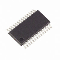
DS3882E+C Maxim Integrated Products, DS3882E+C Datasheet - Page 4

DS3882E+C
Manufacturer Part Number
DS3882E+C
Description
IC CCFL CNTRLR DUAL 28TSSOP
Manufacturer
Maxim Integrated Products
Type
CCFL Controllerr
Datasheet
1.DS3882EC.pdf
(31 pages)
Specifications of DS3882E+C
Frequency
40 ~ 100 kHz
Current - Supply
12mA
Voltage - Supply
4.75 V ~ 5.25 V
Operating Temperature
-40°C ~ 105°C
Package / Case
28-TSSOP
Maximum Operating Temperature
+ 105 C
Mounting Style
SMD/SMT
Minimum Operating Temperature
- 40 C
Lead Free Status / RoHS Status
Lead free / RoHS Compliant
Current - Output
-
Lead Free Status / Rohs Status
Lead free / RoHS Compliant
Other names
Q3390330
Dual-Channel Automotive CCFL Controller
NONVOLATILE MEMORY CHARACTERISTICS
(V
I
(V
Note 1: All voltages are referenced to ground unless otherwise noted. Currents into the IC are positive, out of the IC negative.
Note 2: During fault conditions, the AC-coupled feedback values are allowed to be below the absolute max rating of the LCM or
Note 3: Voltage with respect to V
Note 4: Lamp overdrive and analog dimming (based on reduction of lamp current) are disabled.
Note 5: This is the minimum pulse width guaranteed to generate an output burst, which generates the DS3882’s minimum burst
Note 6: This is the maximum lamp frequency duty cycle that is generated at any of the GAn or GBn outputs with spread-spectrum
Note 7: I
Note 8: After this period, the first clock pulse can be generated.
Note 9: C
Note 10: EEPROM write time applies to all the EEPROM memory. EEPROM write begins after a stop condition occurs.
Note 11: Guaranteed by design.
4
2
EEPROM Write Cycles
SCL Clock Frequency
Bus Free Time Between Stop and
Start Conditions
Hold Time (Repeated) Start
Condition
Low Period of SCL
High Period of SCL
Data Hold Time
Data Setup Time
Start Setup Time
SDA and SCL Rise Time
SDA and SCL Fall Time
Stop Setup Time
SDA and SCL Capacitive
Loading
EEPROM Write Time
CC
CC
C AC ELECTRICAL CHARACTERISTICS (See Figure 9)
_____________________________________________________________________
= +4.75V to 5.25V)
= +4.75V to +5.25V, T
OVD pin for up to 1 second.
duty cycle. This duty cycle may be greater than the duty cycle of the PSYNC input. Once the duty cycle of the PSYNC
input is greater than the DS3882’s minimum duty cycle, the output’s duty cycle tracks the PSYNC’s duty cycle. Leaving
PSYNC low (0% duty cycle) disables the GAn and GBn outputs in DPWM receiver mode.
modulation disabled.
dard-mode timing.
2
PARAMETER
PARAMETER
C interface timing shown is for fast-mode (400kHz) operation. This device is also backward compatible with I
B
—total capacitance allowed on one bus line in picofarads.
A
= -40°C to +105°C, timing referenced to V
DCB
SYMBOL
SYMBOL
t
t
t
t
.
t
HD:DAT
HD:STA
SU:DAT
SU:STA
SU:STO
t
t
f
t
HIGH
LOW
SCL
BUF
C
t
t
t
W
R
F
B
+85°C (Note 11)
(Note 7)
(Note 8)
(Note 9)
(Note 9)
(Note 9)
(Note 10)
CONDITIONS
CONDITIONS
IL(MAX)
and V
IH(MIN)
.)
30,000
0.1C
0.1C
MIN
MIN
20+
20+
100
1.3
0.6
1.3
0.6
0.6
0.6
0
0
B
B
TYP
TYP
20
MAX
MAX
400
300
300
400
0.9
30
2
UNITS
UNITS
C stan-
kHz
ms
pF
µs
µs
µs
µs
µs
ns
µs
ns
ns
µs


