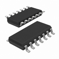
UBA2021T/N2,512 NXP Semiconductors, UBA2021T/N2,512 Datasheet - Page 7

UBA2021T/N2,512
Manufacturer Part Number
UBA2021T/N2,512
Description
IC DRIVER BALLAST CFL/TL 14SOIC
Manufacturer
NXP Semiconductors
Type
CFL/TL Driverr
Datasheet
1.UBA2021PN2112.pdf
(16 pages)
Specifications of UBA2021T/N2,512
Package / Case
14-SOIC (3.9mm Width), 14-SOL
Frequency
41.21 ~ 44.59kHz
Current - Supply
1mA
Voltage - Supply
630V
Operating Temperature
-40°C ~ 150°C
Driver Type
CFL, Fluorescent TL Drivers
Operating Supply Voltage
630 V
Maximum Operating Temperature
+ 150 C
Mounting Style
SMD/SMT
Maximum Output Current
35 mA
Maximum Power Dissipation
500 mW
Minimum Operating Temperature
- 40 C
Supply Current
1 mA
Lead Free Status / RoHS Status
Lead free / RoHS Compliant
Current - Output
-
Lead Free Status / Rohs Status
Lead free / RoHS Compliant
Other names
568-3323-5
935211250512
UBA2021T/N2
935211250512
UBA2021T/N2
Available stocks
Company
Part Number
Manufacturer
Quantity
Price
Part Number:
UBA2021T/N2,512
Manufacturer:
NXP/恩智浦
Quantity:
20 000
NXP Semiconductors
8. Limiting values
UBA2021_4
Product data sheet
7.12 Frequency and change in frequency
7.13 Ground pins
7.14 Charge coupling
At any point in time during oscillation, the circuit will operate between f
change in frequency will be gradual, no steps in frequency will occur. Changes in
frequency caused by a change in voltage at the CI-pin show a rather constant f/ t over
the entire frequency range. The following rates are realized (at a frequency of 85 kHz and
with a 100 nF capacitor connected to the PCI-pin):
The PGND-pin is the ground reference of the IC with respect to the application. As an
exception the SGND-pin provides a local ground reference for the components connected
to the CP-pin, CI-pin, RREF-pin and thee CF-pin. For this purpose the PGND-pin and
SGND-pin are short circuited internally. External connection of the PGND-pin and the
SGND-pin is not preferred. The sum of currents flowing out of the CP-pin, CI-pin,
RREF-pin, CF-pin and the SGND-pin must remain zero at all time.
Due to parasitic capacitive coupling to the high voltage circuitry, all pins are burdened with
a repetitive charge injection. Given the typical application in
the CF-pin are sensitive to this charge injection. For the rating Q
operation of the IC is guaranteed, independent of the current level. Charge coupling at
current levels below 50 mA will not interfere with the accuracy of the V
levels. Charge coupling at current levels below 20 mA will not interfere with the accuracy
of any parameter.
Table 5.
In accordance with the Absolute Maximum Rating System (IEC 60134). All voltages referenced to
ground.
Symbol
V
I
V
SR
P
T
T
VS(clamp)
•
•
•
amb
j
FS
RS
For any increase in frequency: f/ t is between 15 kHz/ms and 37.5 kHz/ms.
During preheat and normal operation: f/ t for a decrease in frequency is between
During the ignition phase: f/ t for a decrease in frequency is between
6 kHz/ms and 15 kHz/ms.
150 Hz/ms and 375 Hz/ms.
Limiting values
Parameter
high side floating supply
voltage
clamp current
input voltage pin RS
slew rate at pins S1, G1
and FS (with respect to
ground)
power dissipation
ambient temperature
junction temperature
Rev. 04 — 25 July 2008
Conditions
operating
t
transient of 50 ns
0.5 s
630 V driver IC for CFL and TL lamps
Figure
Min
-
-
-
-
2.5
15
4
40
40
couple
7, the RREF-pin and
UBA2021
a safe functional
RS(cap)
B
© NXP B.V. 2008. All rights reserved.
Max
570
630
35
+2.5
+2.5
+4
500
+150
+150
and f
and V
start
. Any
Unit
V
V
mA
V
V
V/ns
mW
RS(ctrl)
C
C
7 of 16


