IR21592SPBF International Rectifier, IR21592SPBF Datasheet - Page 2
IR21592SPBF
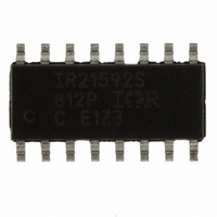
Manufacturer Part Number
IR21592SPBF
Description
IC CNTRLR BALLAST DIMMING 16SOIC
Manufacturer
International Rectifier
Type
Ballast Controllerr
Datasheet
1.IR21592SPBF.pdf
(26 pages)
Specifications of IR21592SPBF
Frequency
73 ~ 108 kHz
Current - Supply
10mA
Voltage - Supply
12.5 V ~ 15.6 V
Operating Temperature
-40°C ~ 125°C
Package / Case
16-SOIC (3.9mm Width)
Package
16-lead SOIC Narrow
Circuit
Fluorescent Ballast IC
Offset Voltage (v)
600
Output Source Current Min (ma)
null
Output Sink Current Min (ma)
null
Vcc Range (v)
12-25V with UVLO
Output Voltage Min (v)
10
Output Voltage Max (v)
20
Pbf
PbF Option Available
For Use With
IRPLDIM2U - BALLAST DIM DIG 32W/T8 120VAC
Lead Free Status / RoHS Status
Lead free / RoHS Compliant
Current - Output
-


IR21592/IR21593
Note 1:
Absolute Maximum Ratings
Absolute maximum ratings indicate sustained limits beyond which damage to the device may occur. All voltage
parameters are absolute voltages referenced to COM, all currents are defined positive into any lead. The thermal
resistance and power dissipation ratings are measured under board mounted and still air conditions.
Symbol
2
I
V
V
Rth
dV/dt
OMAX
I
V
V
V
V
V
V
CPH
I
I
P
V
V
VCO
MAX
T
T
SD
CC
T
DIM
MIN
IPH
HO
CS
LO
B
S
D
S
L
J
JA
This IC contains a zener clamp structure between the chip V
voltage of 15.6V (V
power source greater than the diode clamp voltage (V
section.
Definition
High side floating supply voltage
High side floating supply offset voltage
High side floating output voltage
Low side output voltage
Maximum allowable output current (either output)
due to external power transistor miller effect
Voltage controlled oscillator input voltage
CPH current
IPH voltage
Dimming control pin input voltage
Maximum lamp power setting pin input voltage
Minimum lamp power setting pin input voltage
Current sense input voltage
Shutdown pin current
Supply current (note 1)
Allowable offset voltage slew rate
Package power dissipation @ T
Thermal resistance, junction to ambient
Junction temperature
Storage temperature
Lead temperature (soldering, 10 seconds)
P
D =
(T
JMAX
-T
CLAMP
A
)/Rth
JA
). Please note that this supply pin should not be driven by a DC, low impedance
( S ) & ( PbF )
A
+25°C
(16 pin SOIC)
(16 pin SOIC)
(16 pin DIP)
(16 pin DIP)
CLAMP
CC
) as specified in the Electrical Characteristics
and COM which has a nominal breakdown
V
V
Min.
S
-500
B
-0.3
-0.3
-0.3
-0.3
-0.3
-0.3
-0.3
-0.3
-50
-55
-55
-5
—
—
-5
—
—
—
—
- 0.3
- 25
V
V
V
CC
Max.
B
B
1.60
1.25
625
500
300
115
150
150
6.0
5.5
5.5
5.5
5.5
5.5
25
50
75
+ 0.3
5
5
+ 25
+ 0.3
www.irf.com
Units
V/ns
o
mA
mA
mA
C/W
o
W
V
V
C
V
Related parts for IR21592SPBF
Image
Part Number
Description
Manufacturer
Datasheet
Request
R

Part Number:
Description:
IC CTRLR BALLAST DIMMING 16-DIP
Manufacturer:
International Rectifier
Datasheet:

Part Number:
Description:
IR21592 Dimming Ballast Control IC Design Kit
Manufacturer:
IRF [International Rectifier]
Part Number:
Description:
IC BALLAST CONTROL DIM 16-DIP
Manufacturer:
International Rectifier
Datasheet:
Part Number:
Description:
(IR2159 / IR21591) DIMMING BALLAST CONTROL IC
Manufacturer:
International Rectifier

Part Number:
Description:
SCHOTTKY RECTIFIER
Manufacturer:
International Rectifier Corp.
Datasheet:
Part Number:
Description:
SCHOTTKY RECTIFIER
Manufacturer:
International Rectifier Corp.
Datasheet:
Part Number:
Description:
SCHOTTKY RECTIFIER
Manufacturer:
International Rectifier Corp.
Datasheet:
Part Number:
Description:
SCHOTTKY RECTIFIER
Manufacturer:
International Rectifier Corp.
Datasheet:
Part Number:
Description:
SCHOTTKY RECTIFIER
Manufacturer:
International Rectifier Corp.
Datasheet:
Part Number:
Description:
SCHOTTKY RECTIFIER
Manufacturer:
International Rectifier Corp.
Datasheet:
Part Number:
Description:
SCHOTTKY RECTIFIER
Manufacturer:
International Rectifier Corp.
Datasheet:
Part Number:
Description:
SCHOTTKY RECTIFIER
Manufacturer:
International Rectifier Corp.
Datasheet:
Part Number:
Description:
SCHOTTKY RECTIFIER
Manufacturer:
International Rectifier Corp.
Datasheet:
Part Number:
Description:
SCHOTTKY RECTIFIER
Manufacturer:
International Rectifier Corp.
Datasheet:
Part Number:
Description:
SCHOTTKY RECTIFIER
Manufacturer:
International Rectifier Corp.
Datasheet: