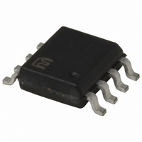
MIC4103YM Micrel Inc, MIC4103YM Datasheet - Page 12

MIC4103YM
Manufacturer Part Number
MIC4103YM
Description
IC MOSFET DRIVER 100V CMOS 8SOIC
Manufacturer
Micrel Inc
Specifications of MIC4103YM
Configuration
Half Bridge
Input Type
Non-Inverting
Delay Time
24ns
Current - Peak
2A
Number Of Configurations
1
Number Of Outputs
2
High Side Voltage - Max (bootstrap)
118V
Voltage - Supply
9 V ~ 16 V
Operating Temperature
-40°C ~ 125°C
Mounting Type
Surface Mount
Package / Case
8-SOIC (3.9mm Width)
Device Type
MOSFET
Module Configuration
Half Bridge
Peak Output Current
3A
Output Resistance
2.5ohm
Input Delay
24ns
Output Delay
24ns
Supply Voltage Range
9V To 16V
Driver Case
RoHS Compliant
Lead Free Status / RoHS Status
Lead free / RoHS Compliant
Other names
576-1589
and gate to drain capacitance of the external MOSFET.
Figure 7 shows a simplified equivalent circuit of the
MIC4103 driving an external MOSFET.
Dissipation during the external MOSFET Turn-On
Energy from capacitor C
capacitance of the MOSFET (C
delivered to the MOSFET is dissipated in the three
resistive components, R
resistance of the upper driver MOSFET in the MIC4103.
R
the MOSFET. R
MOSFET. R
specifications. The ESR of capacitor C
of the connecting trace can be ignored since they are
much less than R
The effective capacitance of C
calculate since they vary non-linearly with I
Fortunately, most power MOSFET specifications include a
typical graph of total gate charge vs. V
a typical gate charge curve for an arbitrary power
MOSFET. This chart shows that for a gate voltage of 10V,
the MOSFET requires about 23.5nC of charge. The energy
dissipated by the resistive components of the gate drive
circuit during turn-on is calculated as:
Micrel
October 2007
G
C
B
is the series resistor (if any) between the driver IC and
Figure 7. MIC4103 Driving an External MOSFET
E
but
Q
E
where
Ciss
so
=
=
=
1/2
C
1
2
is
×
×
the
×
Ciss
V
G_FET
Qg
total
Vdd
×
×
ON
is usually listed in the power MOSFET’s
V
V
G_FET
gs
gate
gs
and R
Roff
Ron
2
HS
capacitanc
ON
is the gate resistance of the
B
HB
G_FET
, R
is used to charge up the input
HO
G
, and R
.
Rg
GD
GD
e
and C
and C
Rg_fet
of
G_FET
B
Cgd
the
GS
Cgs
and the resistance
External
. Figure 8 shows
GS
GS
D
FET
MOSFET
. R
, V
). The energy
is difficult to
ON
GS
, and V
is the on
DS
.
12
The same energy is dissipated by R
when the driver IC turns the MOSFET off. Assuming R
approximately equal to Roff, the total energy and power
dissipated by the resistive drive elements is:
The power dissipated inside the MIC4103/4 is equal to the
ratio of R
and R
MIC4103 due to driving the external MOSFET is:
Supply Current Power Dissipation
Power is dissipated in the MIC4103 even if there is nothing
being driven. The supply current is drawn by the bias for
the internal circuitry, the level shifting circuitry, and shoot-
through current in the output drivers. The supply current is
proportional to operating frequency and the V
voltages. The typical characteristic graphs show how
supply current varies with switching frequency and supply
voltage.
The power dissipated by the MIC4103 due to supply
current is:
E
and
P
where
E
P
Q
fs
V
Pdiss
Pdiss
driver
driver
driver
driver
GS
G
is
G_FET
is
the
is
the
Figure 8. Typical Gate Charge vs. V
is
is
the
ON
=
=
drive
sup
switching
. Letting R
the
Q
the
Q
total
gate
G
& R
G
ply
power
×
energy
×
=
V
V
gate
=
GS
GS
to
OFF
P
driver
V
source
frequency
×
dissipated
DD
charge
dissipated
fs
to the external resistive losses in R
ON
×
R
=R
voltage
I
ON
DD
at
of
OFF
Vgs
by
per
+
the
+
, the power dissipated in the
switching
V
on
R
switching
HB
gate
R
G
the
ON
+
×
MOSFET
drive
R
I
HB
OFF
the
G
cycle
_
circuit
, R
MOSFET
FET
M9999-100107-B
MIC4103/4104
G
, and R
GS
DD
on
and V
and
G_FET
ON
off
HB
is
G


