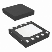
LM5110-3SD/NOPB National Semiconductor, LM5110-3SD/NOPB Datasheet - Page 8

LM5110-3SD/NOPB
Manufacturer Part Number
LM5110-3SD/NOPB
Description
IC DRIVER DUAL 5A NEG VOUT 10LLP
Manufacturer
National Semiconductor
Datasheet
1.LM5110-1MNOPB.pdf
(13 pages)
Specifications of LM5110-3SD/NOPB
Configuration
Low-Side
Input Type
Inverting and Non-Inverting
Delay Time
25ns
Current - Peak
5A
Number Of Configurations
2
Number Of Outputs
2
Voltage - Supply
3.5 V ~ 14 V
Operating Temperature
-40°C ~ 125°C
Mounting Type
Surface Mount
Package / Case
10-LLP
Lead Free Status / RoHS Status
Lead free / RoHS Compliant
High Side Voltage - Max (bootstrap)
-
Other names
LM5110-3SD
LM5110-3SDTR
LM5110-3SDTR
www.national.com
Typical Performance Characteristics
Detailed Operating Description
LM5110 dual gate driver consists of two independent and
identical driver channels with TTL compatible logic inputs
and high current totem-pole outputs that source or sink
current to drive MOSFET gates. The driver output consist of
a compound structure with MOS and bipolar transistor oper-
ating in parallel to optimize current capability over a wide
output voltage and operating temperature range. The bipolar
device provides high peak current at the critical threshold
region of the MOSFET VGS while the MOS devices provide
rail-to-rail output swing. The totem pole output drives the
MOSFET gate between the gate drive supply voltage V
and the power ground potential at the V
The control inputs of the drivers are high impedance CMOS
buffers with TTL compatible threshold voltages. The nega-
tive supply of the input buffer is connected to the input
ground pin IN_REF. An internal level shifting circuit connects
the logic input buffers to the totem pole output drivers. The
level shift circuit and separate input/output ground pins pro-
vide the option of single supply or split supply configurations.
When driving MOSFET gates from a single positive supply,
the IN_REF and V
Delay Time vs Temperature
EE
pins are both connected to the power
UVLO Thresholds and Hysteresis vs Temperature
EE
pin.
20079216
CC
8
(Continued)
ground. The LM5110 pinout was designed for compatibility
with industry standard gate drivers in single supply gate
driver applications. Pin 1 (IN_REF) on the LM5110 is a
no-connect on standard driver IC’s. Connecting pin 1 to pin 3
(V
of both the LM5110 and competitive drivers.
The isolated input/output grounds provide the capability to
drive the MOSFET to a negative VGS voltage for a more
robust and reliable off state. In split supply configuration, the
IN_REF pin is connected to the ground of the controller
which drives the LM5110 inputs. The V
a negative bias supply that can range from the IN-REF as
much as 14V below the V
mum recommended voltage difference between V
IN_REF or between V
voltage difference between V
Enhancement mode MOSFETs do not inherently require a
negative bias on the gate to turn off the FET. However,
certain applications may benefit from the capability of nega-
tive VGS voltage during turn-off including:
1. when the gate voltages cannot be held safely below the
EE
threshold voltage due to transients or coupling in the
printed circuit board.
) on the printed circuit board accommodates the pin-out
RDSON vs Supply Voltage
20079218
CC
CC
and V
CC
gate drive supply. The maxi-
and IN_REF is 3.5V.
EE
is 14V. The minimum
EE
pin is connected to
20079217
CC
and


