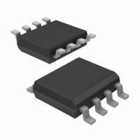
IR2153SPBF International Rectifier, IR2153SPBF Datasheet - Page 4

IR2153SPBF
Manufacturer Part Number
IR2153SPBF
Description
IC DRIVER HALF BRIDGE OSC 8SOIC
Manufacturer
International Rectifier
Datasheet
1.IR2153SPBF.pdf
(9 pages)
Specifications of IR2153SPBF
Configuration
High and Low Side, Synchronous
Input Type
Self Oscillating
Current - Peak
200mA
Number Of Configurations
1
Number Of Outputs
2
High Side Voltage - Max (bootstrap)
600V
Voltage - Supply
10 V ~ 15.6 V
Operating Temperature
-40°C ~ 125°C
Mounting Type
Surface Mount
Package / Case
8-SOIC (3.9mm Width)
Current, Leakage, Offset
50 UA
Current, Supply
25 mA
Driver Type
Half Bridge
Package Type
SOIC
Power Dissipation
0.625 W
Temperature, Operating, Maximum
+150
Temperature, Operating, Minimum
-55
Thermal Resistance, Junction To Ambient
200 degC/W
Time, Fall, Turn-off
100 ns
Time, Rise, Turn-on
150 ns
Voltage, Offset
600 V
Lead Free Status / RoHS Status
Lead free / RoHS Compliant
Delay Time
-
Lead Free Status / Rohs Status
RoHS Compliant part
Available stocks
Company
Part Number
Manufacturer
Quantity
Price
Part Number:
IR2153SPBF
Manufacturer:
IR
Quantity:
20 000
NOTE:For new designs, we recommend
IR’s new product IRS2153D
IR2153(D)(S) & (PbF)
Oscillator I/O Characteristics
Electrical Characteristics
V
parameters are referenced to COM. The V
respective output leads: HO or LO.
Low Voltage Supply Characteristics
Floating Supply Characteristics
V
I
I
I
V
Symbol Definition
I
V
V
V
Symbol Definition
I
V
V
V
V
I
Symbol Definition
f osc
d
V
V
V
I
V
QBSUV
QBS
LK
CTUV
CT
BIAS
QCC
QCCUV
BSMIN
F
CTSD
RTUV
RTSD
CT+
CT-
RT+
RT-
4
CCUV+
CCUV-
CCUVH
CLAMP
(V
CC
R
UV-mode C
Upper C
Lower C
C
High-level R
Low-level R
UV-mode R
SD-Mode R
Oscillator frequency
C
, V
Quiescent VBS supply current
Minimum required V
functionality from R
Offset supply leakage current
Bootstrap diode forward voltage (IR2153D)
T
Rising V
Falling V
V
Micropower startup V
Quiescent V
V
Micropower startup V
T
T
pin duty cycle
CC
CC
BS
voltage shutdown threshold
pin current
) = 12V, C
undervoltage lockout Hysteresis
zener clamp voltage
T
T
CC
CC
ramp voltage threshold
ramp voltage threshold
T
T
T
T
T
undervoltage lockout threshold
undervoltage lockout threshold
output voltage
output voltage, V
CC
pin pulldown current
output voltage
output voltage, V
L
supply current
= 1000 pF, C
T
BS
to HO
CC
BS
voltage for proper
supply current
supply current
CC
CC
T
O
= 1 nF and T
- V
- V
and I
RT
RT
O
parameters are referenced to COM and are applicable to the
A
= 25°C unless otherwise specified. The V
Min.
Min.
Min.
19.4
0.30
14.4
1.8
8.1
7.2
0.5
94
48
—
—
—
—
—
—
—
—
—
—
—
—
—
—
—
—
0.5
Typ.
0.001
Typ.
Typ.
100
0.70
100
100
15.6
50
10
10
10
500
20
8.0
4.0
2.1
10
1.0
4.0
9.0
8.0
0
75
30
—
—
0
Max.
Max.
Max.
16.8
20.6
150
950
106
1.5
9.9
8.8
52
1.0
1.2
—
—
2.4
50
300
50
300
100
50
300
5.0
10
50
50
1.0
Units
Units Test Conditions
Units Test Conditions
kHz
mV
%
uA
mA
V
μA
V
μA
μA
V
V
V
Test Conditions
V
IN
CC
R
R
fo < 100kHz
V
I
I
I
I
V
I
V
I
V
V
I
V
V
I
, V
RT
RT
RT
RT
RT
RT
CC
F
CC
CC
CT
CT
CC
T
T
CC
B
=V
= 250mA
TH
= 36.9kΩ
= 7.43kΩ
= V
= 100μA
= 100μA
= 1mA
= 1mA
= 100μA,
= 1mA,
= 5mA
≤ V
= 0V
= 0V
≤ V
= 7V
≤ V
CCUV+
and I
www.irf.com
S
CCUV
CCUV
CCUV
= 600V
IN
+ 0.1V
-
-
-


