IRS2103PBF International Rectifier, IRS2103PBF Datasheet - Page 2
IRS2103PBF
Manufacturer Part Number
IRS2103PBF
Description
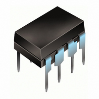
IC DRIVER HALF-BRIDGE 8-DIP
Manufacturer
International Rectifier
Datasheet
1.IRS2103PBF.pdf
(14 pages)
Specifications of IRS2103PBF
Configuration
Half Bridge
Input Type
Inverting and Non-Inverting
Delay Time
680ns
Current - Peak
290mA
Number Of Configurations
1
Number Of Outputs
2
High Side Voltage - Max (bootstrap)
600V
Voltage - Supply
10 V ~ 20 V
Operating Temperature
-40°C ~ 125°C
Mounting Type
Through Hole
Package / Case
8-DIP (0.300", 7.62mm)
Family Hvic
General Purpose HVICs
Channels
2
Topology
Half Bridge
Application
General Purpose / Motor Control
Voffset
600
Io+ (ma)
290
Io- (ma)
600
Uvlo
Vcc
Vbsuv+ / Vccuv+ Min (v)
8.0
Vbsuv+ / Vccuv+ Typ (v)
8.9
Vbsuv+ / Vccuv+ Max (v)
9.8
Vbsuv- / Vccuv- Min (v)
7.4
Vbsuv- / Vccuv- Typ (v)
8.2
Vbsuv- / Vccuv- Max (v)
9.0
Dt / Sdt Min (ns)
400
Dt / Sdt Typ (ns)
520
Dt / Sdt Max (ns)
650
T On Typ (ns)
680
T On Max (ns)
820
T Off Typ (ns)
150
T Off Max (ns)
220
Inverter Input Logic
LIN
Package
8 Lead
Part Status
Active & Preferred
Lead Free Status / RoHS Status
Lead free / RoHS Compliant
Available stocks
Company
Part Number
Manufacturer
Quantity
Price
Company:

Part Number:
IRS2103PBF
Manufacturer:
IR
Quantity:
20 753


www.irf.com
Absolute Maximum Ratings
Absolute maximum ratings indicate sustained limits beyond which damage to the device may occur. All voltage param-
eters are absolute voltages referenced to COM. The thermal resistance and power dissipation ratings are measured
under board mounted and still air conditions.
Recommended Operating Conditions
The input/output logic timing diagram is shown in Fig. 1. For proper operation the device should be used within the
recommended conditions. The V
Note 1: Logic operational for V
DT97-3 for more details).
Symbol
Symbol
dV s /dt
Rth
V
V
V
V
V
V
V
V
V
V
P
T
V
V
T
T
T
HO
HO
CC
CC
LO
LO
IN
IN
D
A
B
S
J
S
L
B
S
JA
High-side floating absolute voltage
High-side floating supply offset voltage
High-side floating output voltage
Low-side and logic fixed supply voltage
Low-side output voltage
Logic input voltage (HIN & LIN )
Allowable offset supply voltage transient
Package power dissipation @ T
Thermal resistance, junction to ambient
Junction temperature
Storage temperature
Lead temperature (soldering, 10 seconds)
High-side floating supply absolute voltage
High-side floating supply offset voltage
High-side floating output voltage
Low-side and logic fixed supply voltage
Low-side output voltage
Logic input voltage (HIN & LIN )
Ambient temperature
S
S
of -5 V to +600 V. Logic state held for V
offset rating is tested with all supplies biased at a 15 V differential.
Definition
Definition
A
+25 °C
(8 Lead PDIP)
(8 Lead SOIC)
(8 Lead PDIP)
(8 Lead SOIC)
S
of -5 V to -V
V
V
V
Note 1
Min.
Min.
IRS2103(S)PbF
S
S
B
-0.3
-0.3
-0.3
-0.3
-55
-40
V
—
—
—
—
—
—
—
10
0
BS
- 0.3
+ 10
0
- 25
S
. (Please refer to the Design Tip
V
V
V
V
V
CC
CC
Max.
Max.
0.625
B
B
S
V
V
125
200
150
150
300
600
125
625
1.0
V
50
25
20
+ 0.3
+ 0.3
CC
CC
+ 20
+ 0.3
+ 0.3
B
Units
Units
V/ns
°C/W
°C
°C
W
V
V
2
Related parts for IRS2103PBF
Image
Part Number
Description
Manufacturer
Datasheet
Request
R

Part Number:
Description:
HALF-BRIDGE DRIVER
Manufacturer:
IRF [International Rectifier]
Datasheet:

Part Number:
Description:
SCHOTTKY RECTIFIER
Manufacturer:
International Rectifier Corp.
Datasheet:
Part Number:
Description:
SCHOTTKY RECTIFIER
Manufacturer:
International Rectifier Corp.
Datasheet:
Part Number:
Description:
SCHOTTKY RECTIFIER
Manufacturer:
International Rectifier Corp.
Datasheet:
Part Number:
Description:
SCHOTTKY RECTIFIER
Manufacturer:
International Rectifier Corp.
Datasheet:
Part Number:
Description:
SCHOTTKY RECTIFIER
Manufacturer:
International Rectifier Corp.
Datasheet:
Part Number:
Description:
SCHOTTKY RECTIFIER
Manufacturer:
International Rectifier Corp.
Datasheet:
Part Number:
Description:
SCHOTTKY RECTIFIER
Manufacturer:
International Rectifier Corp.
Datasheet:
Part Number:
Description:
SCHOTTKY RECTIFIER
Manufacturer:
International Rectifier Corp.
Datasheet:
Part Number:
Description:
SCHOTTKY RECTIFIER
Manufacturer:
International Rectifier Corp.
Datasheet:
Part Number:
Description:
SCHOTTKY RECTIFIER
Manufacturer:
International Rectifier Corp.
Datasheet:
Part Number:
Description:
SCHOTTKY RECTIFIER
Manufacturer:
International Rectifier Corp.
Datasheet:
Part Number:
Description:
SCHOTTKY RECTIFIER
Manufacturer:
International Rectifier Corp.
Datasheet:
Part Number:
Description:
SCHOTTKY RECTIFIER
Manufacturer:
International Rectifier Corp.
Datasheet:
Part Number:
Description:
SCHOTTKY RECTIFIER
Manufacturer:
International Rectifier Corp.
Datasheet: