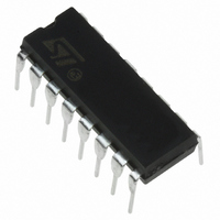
TD310IN STMicroelectronics, TD310IN Datasheet - Page 3

TD310IN
Manufacturer Part Number
TD310IN
Description
IC IGBT/MOS DRIVER TRPL 16-DIP
Manufacturer
STMicroelectronics
Type
Low Sider
Datasheet
1.TD310ID.pdf
(9 pages)
Specifications of TD310IN
Configuration
Multiple
Input Type
Non-Inverting
Delay Time
200ns
Current - Peak
600mA
Number Of Configurations
3
Number Of Outputs
3
Voltage - Supply
4 V ~ 16 V
Operating Temperature
-40°C ~ 125°C
Mounting Type
Through Hole
Package / Case
16-DIP (0.300", 7.62mm)
Supply Voltage (min)
4 V
Supply Current
2 mA
Maximum Operating Temperature
+ 125 C
Mounting Style
Through Hole
Bridge Type
Half Bridge
Minimum Operating Temperature
- 40 C
Number Of Drivers
3
Output Current
250 mA
Lead Free Status / RoHS Status
Lead free / RoHS Compliant
High Side Voltage - Max (bootstrap)
-
Lead Free Status / Rohs Status
Lead free / RoHS Compliant
Other names
497-7649-5
TD310IN
TD310IN
Available stocks
Company
Part Number
Manufacturer
Quantity
Price
Company:
Part Number:
TD310IN
Manufacturer:
BCD
Quantity:
15 000
ELECTRICAL CHARACTERISTICS
V
LOGIC INPUT (all inputs)
OUTPUT DRIVERS
ALARM OUTPUT
SENSE INPUT
OPERATIONAL AMPLIFIER
STAND-BY
UNDER VOLTAGE LOCKOUT
Symbol
CC
t
t
V
dH
dL
V
GBP
V
R
I
V
V
V
V
V
V
V
A
SR
stdby
I
V
V
I
I
t
I
stdby
I
t
= 15V, T
CC
, t
t
t
shys
t
dem
I
t
adj
IH
, t
dd
sod
opd
sh
icm
hys
IL
Ai
sid
A
ios
si
st1
IH
li
s
s
vd
IL
io
eH
eL
Supply Current with Inputs in High State
High Input Voltage
Low Input Voltage
High Input Current
Low Input Current
Propagation Delay (10% input to 10% output)
Input Inhibiting Time
Differential Delay Time Between Channels
Sourcing Drop Voltage (A/B/C outputs)
Sinking Drop Voltage (A/B/C outputs)
Demagnetizing Drop Voltage (A/B/C outputs)
Output Pull Down Resistor
Low Level Sinking Current
High Level Sinking Current
Alarm Output : Delay Time to Alarm Fall if Sense Input Triggered
Input Offset Voltage
Inhibition Time if Sense Input Triggered
Delay Time to Output Fall if Sense Input Triggered
Inhibition Time of Sense Input
Sense Hysteresis
Common Mode Input Voltage Range
Input Offset Voltage
Gain Bandwidth Product
Open Loop Gain
Slew Rate at Unity Gain (R
Standby Mode Threshold Voltage
Standby Mode Supply Current
Under Voltage Level Adjust Current
Internal Stop Threshold (without external adjustment)
Threshold Hysteresis
amb
= 25°C (unless otherwise specified)
Output Delay
Output Delay
T
I
Isink = 200mA
Idemag. = 100mA
V
All outputs inhibited
source
min.
O
= 0.8V
= 200mA
Tamb
T
max.
L
= 100k , C
Parameter
L
= 100pF, V
i
= 3 to 7V)
Min.
10.7
0.3
60
2
5
0 to V
Typ.
200
100
300
1.5
0.6
0.8
10
10
60
20
47
35
40
CC
30
1
1
1
+
- 1.5
Max.
13.3
400
400
500
600
0.8
1.1
20
10
2
3
5
2
1
TD310
Unit
MHz
V/ s
mA
mA
mV
mV
mV
ms
pA
pA
k
dB
ns
ns
ns
ns
ns
ns
A/V
V
V
V
V
V
V
V
V
V
A
A
3/9


