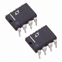
LTC1154CN8 Linear Technology, LTC1154CN8 Datasheet - Page 5

LTC1154CN8
Manufacturer Part Number
LTC1154CN8
Description
IC MOSFET DRIVER HIGH-SIDE 8-DIP
Manufacturer
Linear Technology
Datasheet
1.LTC1154CS8PBF.pdf
(18 pages)
Specifications of LTC1154CN8
Configuration
High-Side
Input Type
Inverting
Delay Time
160µs
Number Of Configurations
1
Number Of Outputs
1
Voltage - Supply
4.5 V ~ 18 V
Operating Temperature
0°C ~ 70°C
Mounting Type
Through Hole
Package / Case
8-DIP (0.300", 7.62mm)
Lead Free Status / RoHS Status
Contains lead / RoHS non-compliant
Current - Peak
-
High Side Voltage - Max (bootstrap)
-
Available stocks
Company
Part Number
Manufacturer
Quantity
Price
Company:
Part Number:
LTC1154CN8
Manufacturer:
LT
Quantity:
5 510
Company:
Part Number:
LTC1154CN8
Manufacturer:
SHARP
Quantity:
5 510
TYPICAL PERFORMANCE CHARACTERISTICS
PIN FUNCTIONS
Input and Shutdown Pins
The LTC1154 input pin is active high and activates all of the
protection and charge pump circuitry when switched ON.
The shutdown pin is designed to immediately disable the
switch if a secondary fault condition (over temperature,
etc.) is detected. The LTC1154 logic and shutdown inputs
are high impedance CMOS gates with ESD protection
diodes to ground and supply and therefore should not be
forced beyond the power supply rails. The shutdown pin
should be connected to ground when not in use.
2.4
2.2
2.0
1.8
1.6
1.4
1.2
1.0
0.8
0.6
0.4
30
50
45
40
35
25
20
15
10
0
5
–50
–50
Standby Supply Current
Shutdown Threshold Voltage
V
V
IN
EN
–25
–25
= 0V
= 0V
0
0
TEMPERATURE (°C)
TEMPERATURE (°C)
25
25
V
V
50
50
S
S
= 5V
= 18V
V
V
S
S
75
= 5V
= 18V
75
LTC1154 • TPC13
LTC1154 • TPC10
100
100
125
125
1000
900
800
700
600
500
400
300
200
100
5.0
4.5
4.0
3.5
3.0
2.5
2.0
1.5
1.0
0.5
0
0
–50
–50
Supply Current ON
ENABLE Threshold Voltage
V
V
V
S
IN
EN
–25
–25
= 12V
V
= 5V
= 0V
V
S
S
= 12V
= 5V
0
0
TEMPERATURE (°C)
TEMPERATURE (°C)
25
25
DISABLE
ENABLE
ENABLE Input Pin
The ENABLE input can be used to enable a number of
LTC1154 high side switches in banks or to provide a sec-
ondary means of control. It can also act as an inverting
input. The ENABLE input is a high impedance CMOS gate
with ESD clamp diodes to ground and supply and therefore
should not be forced beyond the power supply rails. This
pin should be grounded when not in use.
50
50
75
75
LTC1154 • TPC11
LTC1154 • TPC14
100
100
125
125
1000
100
0.1
2.4
2.2
2.0
1.8
1.6
1.4
1.2
1.0
0.8
0.6
0.4
10
1
–50
0
Input ON Threshold Voltage
Gate Drive Current
T
A
= 25°C
–25
GATE VOLTAGE ABOVE SUPPLY (V)
V
S
4
= 5V
0
TEMPERATURE (°C)
V
8
25
S
= 12V
LTC1154
V
V
50
S
S
12
= 5V
= 18V
V
S
75
= 18V
16
LTC1154 • TPC12
LTC1154 • TPC15
100
1154fb
5
125
20


