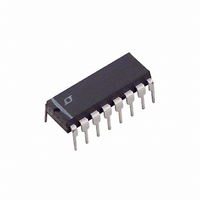
LT1336IN Linear Technology, LT1336IN Datasheet - Page 11

LT1336IN
Manufacturer Part Number
LT1336IN
Description
IC MOSFET DRVR 1/2BRDG NCH 16DIP
Manufacturer
Linear Technology
Datasheet
1.LT1336CSPBF.pdf
(20 pages)
Specifications of LT1336IN
Configuration
Half Bridge
Input Type
Differential
Delay Time
250ns
Current - Peak
1.5A
Number Of Configurations
1
Number Of Outputs
2
High Side Voltage - Max (bootstrap)
60V
Voltage - Supply
10 V ~ 15 V
Operating Temperature
-40°C ~ 85°C
Mounting Type
Through Hole
Package / Case
16-DIP (0.300", 7.62mm)
Lead Free Status / RoHS Status
Contains lead / RoHS non-compliant
Available stocks
Company
Part Number
Manufacturer
Quantity
Price
Part Number:
LT1336IN#PBF
Manufacturer:
LINEAR/凌特
Quantity:
20 000
applicaTions inForMaTion
In applications where switching is always above 10kHz
and the duty cycle never exceeds 90%, Pins 1, 15 and 16
can be left open. The bootstrap capacitor is then charged
by conventional bootstrapping. Only a diode needs to be
connected between V
capacitor is usually adequate using this technique for driv-
ing a single MOSFET under 10,000pF . When driving multiple
MOSFETs in parallel, if the total gate capacitance exceeds
10,000pF , the bootstrap capacitor should be increased
proportionally above 0.1µF (see Paralleling MOSFETs).
Deriving the Floating Supply with the Boost Topology
The advantage of using the boost topology is its simplicity.
Only a resistor, a small inductor, a diode and a capacitor
are needed. However, the high voltage rail may not exceed
40V to avoid reaching the collector-base breakdown volt-
age of the internal NPN switch.
The recommended values for the current sense resistor,
inductor and bootstrap capacitor are 2Ω, 200µH and
1µF respectively. Using the recommended component
values the boost regulator will run at around 700kHz. To
lower the frequency the inductor value can be increased
and to increase the frequency the inductor value can be
decreased. The sense resistor should be at least 1.5Ω to
maintain adequate inductor current limit. The bootstrap
capacitor value should be 1µF or larger to minimize ripple
voltage. An example of a boost regulator is shown in
Figure 1.
* SUMIDA RCR-664D-221KC
R
2
1/4W
SENSE
SV
PV
Figure 1. Using the Boost Regulator
+
+
I
SENSE
LT1336
1N4148
+
TSOURCE
200µH*
TGATEDR
D1
TGATEFB
and the Boost pin. A 0.1µF bootstrap
SWITCH
SWGND
BOOST
S
+
V
–
BOOST
+
D2
1N4148
C
1µF
BOOST
HV = 40V MAX
1336 F01
+
The boost regulator works as follows: when switch S is
on, the inductor current ramps up as the magnetic field
builds up. During this interval energy is being stored in the
inductor and no power is transferred to V
inductor peak current is reached, sensed by the 2Ω resistor,
the switch is turned off. Energy is no longer transferred to
the inductor causing the magnetic field to collapse. The
collapsing magnetic field induces a change in voltage across
the inductor. The Switch pin voltage rises until diode D2
starts conducting. As the inductor current ramps down,
the lower inductor current threshold is reached and switch
S is turned off, thus completing the cycle.
Current drawn from V
this current (~ 1.5mA) flows through the topside driver
to the Top Source pin. This current is typically returned
to ground via the bottom MOSFET or the output load. If
the bottom MOSFET were off and the output load were
returned to HV, then the Top Source pin will return the
current to HV through the top MOSFET or the output load.
If the HV supply cannot sink current and no load draw-
ing greater than 1.5mA is connected to the supply, then
a resistor from HV to ground may be needed to prevent
voltage buildup on the HV supply.
Note that the current drawn from V
V
V
Deriving the Floating Supply with the Flyback
Topology
For applications where the high voltage rail is greater than
40V, the flyback topology must be used. To configure a
flyback regulator, a resistor, a diode, a small 1:1 turns ratio
transformer and a capacitor are needed. The maximum
voltage across the switch, assuming an ideal transformer,
will be about V
transformers will induce an overvoltage spike at the switch
at the instant when it opens. These spikes can be clamped
using a snubbing network or a Zener. Unlike the boost
topology, the current drawn from V
is equal to the current drawn from V
BOOST
BOOST
I
IN V
( )
+
is significantly higher than the current drawn from
as given by:
=I
OUT
+
V
+ 11.3V. Leakage inductance in nonideal
BOOST
V
+
+
is delivered to V
+
BOOST
(assuming no loss)
+
and delivered to
BOOST
BOOST
.
LT1336
. When the
. Some of
11
1336fa


