BUK218-50DC,118 NXP Semiconductors, BUK218-50DC,118 Datasheet
BUK218-50DC,118
Specifications of BUK218-50DC,118
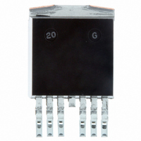
BUK218-50DC /T3
BUK218-50DC /T3


Related parts for BUK218-50DC,118


BUK218-50DC,118 Summary of contents
Page 1
... On-state resistance FUNCTIONAL BLOCK DIAGRAM INPUT 1 INPUT 2 STATUS CONTROL & PROTECTION CIRCUITS GROUND RG Fig.1. Elements of the TOPFET dual HSS with internal ground resistor. PIN CONFIGURATION Fig Product specification BUK218-50DC MIN. UNIT 8 MAX. UNIT 50 16 150 ˚C = 25˚ BATT LOAD 1 LOAD 2 SYMBOL ...
Page 2
... October 2001 CONDITIONS T 135˚ 25˚ limit input, status currents 0. 300 300 150˚C prior to turn-off j CONDITIONS Human body model 250 pF 1 allowed as an overload condition but at the threshold Product specification BUK218-50DC MIN. MAX. UNIT 83.3 W -55 175 ˚C -40 150 ˚ 3 ...
Page 3
... 300 battery to ground - one channel on both channels 0 85˚ -200 mA 300 5 tests are continuous. The specified pulse duration t 3 Product specification BUK218-50DC MIN. TYP. - 2.4 - 1.2 MIN. TYP 5 25˚ 25˚ 1 300 s 25˚ 150˚ 300 s 25˚C ...
Page 4
... CONDITIONS 200 1 25˚C. mb CONDITIONS open circuit detected, other channel off 3 input low to status low = 5 V ext 4 Product specification BUK218-50DC MIN. TYP. MAX. UNIT 20 60 160 A 5 1.2 1 0.15 0.3 0 100 TRUTH TABLE MIN. TYP. MAX. UNIT 1.5 2 ...
Page 5
... 5 125˚C prior to overload mb 4 for protection which determines trip time < P and T < D(TO) j j(TO) according to the exponential model formula Product specification BUK218-50DC . TRUTH TABLE MIN. TYP. MAX. 2 4.2 0 25˚C unless otherwise stated. mb MIN. TYP. MAX 100 150 ...
Page 6
... X OFF OFF OFF OFF OFF OFF OFF undervoltage OV overvoltage OC open circuit SC short circuit OT overtemperature 6 Product specification BUK218-50DC TRUTH TABLE MIN. TYP. MAX. 5.5 7 8.5 - 0 25˚ DESCRIPTION both off & normal both off, one/both OC or short to V+ one off & OC, other on & normal one on & ...
Page 7
... C Input capacitance ig C Output capacitance bl October 2001 = 13 per channel. L CONDITIONS from input going high to 10 30 from input going low to 90 70 CONDITIONS Product specification BUK218-50DC MIN. TYP. MAX. UNIT - 0 100 400 0 200 s MIN. TYP. MAX. UNIT - ...
Page 8
... For soldering guidelines and SMD footprint design, please refer to Data Handbook SC18. October 2001 2 scale max. 0.64 1.60 10.30 2.90 15.80 11 1.27 0.46 2.10 14.80 1.20 9.70 REFERENCES JEDEC EIAJ 1 , centre pin connected to mounting base. 8 Product specification BUK218-50DC 2 -PAK); SOT427 mounting base 2.60 2.20 EUROPEAN ISSUE DATE PROJECTION 99-06-25 01-04-18 Rev 2.010 ...
Page 9
... This data sheet contains data from the product specification. Philips Semiconductors reserves the right to make changes at any time in order to improve the design, manufacturing and supply. Changes will be communicated according to the Customer Product/Process Change Notification (CPCN) procedure SNW-SQ-650A 9 Product specification BUK218-50DC Rev 2.010 ...