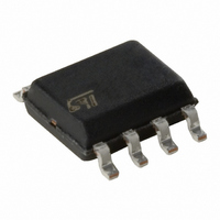
TD352ID STMicroelectronics, TD352ID Datasheet - Page 5

TD352ID
Manufacturer Part Number
TD352ID
Description
IC IGBT/MOSFET DRIVER ADV 8-SOIC
Manufacturer
STMicroelectronics
Type
High Side/Low Sider
Datasheet
1.TD352IDT.pdf
(13 pages)
Specifications of TD352ID
Configuration
Low-Side
Input Type
Non-Inverting
Delay Time
2µs
Current - Peak
750mA
Number Of Configurations
1
Number Of Outputs
1
Voltage - Supply
12 V ~ 26 V
Operating Temperature
-40°C ~ 125°C
Mounting Type
Surface Mount
Package / Case
14-SOIC (3.9mm Width), 14-SOL
Rise Time
100 ns
Fall Time
100 ns
Supply Voltage (min)
12 V
Supply Current
2.5 mA
Maximum Power Dissipation
500 mW
Maximum Operating Temperature
+ 125 C
Mounting Style
SMD/SMT
Bridge Type
Half Bridge
Minimum Operating Temperature
- 40 C
Number Of Drivers
1
Lead Free Status / RoHS Status
Lead free / RoHS Compliant
High Side Voltage - Max (bootstrap)
-
Lead Free Status / Rohs Status
Lead free / RoHS Compliant
Available stocks
Company
Part Number
Manufacturer
Quantity
Price
Part Number:
TD352IDT
Manufacturer:
ST
Quantity:
20 000
Functional Description
4 Functional Description
4.1 Input stage
TD352 IN input is clamped at about 5V to 7V. The input is triggered by the signal edge. When using an
open collector optocoupler, the resistive pull-up resistor can be connected to either VREF or VH.
Recommended pull-up resistor value with VH=16V are from 4.7k to 22k.
4.2 Voltage reference
A voltage reference is used to create accurate timing for the turn-on delay with external resistor and
capacitor. The same circuitry is also used for the two-level turn-off delay.
A decoupling capacitor (10nF to 100nF) on VREF pin is required to ensure good noise rejection.
4.3 Active Miller clamp:
The TD352 offers an alternative solution to the problem of the Miller current in IGBT switching
applications. Instead of driving the IGBT gate to a negative voltage to increase the safety margin, the
TD352 uses a dedicated CLAMP pin to control the Miller current. When the IGBT is off, a low impedance
path is established between IGBT gate and emitter to carry the Miller current, and the voltage spike on
the IGBT gate is greatly reduced.
During turn-off, the gate voltage is monitored and the clamp output is activated when gate voltage goes
below 2V (relative to VL). The clamp voltage is VL+4V max for a Miller current up to 500mA. The clamp
is disabled when the IN input is triggered again.
The CLAMP function doesn’t affect the turn-off characteristic, but only keeps the gate to the low level
throughout the off time. The main benefit is that negative voltage can be avoided in many cases, allowing
a bootstrap technique for the high side driver supply.
4.4 Turn-on delay
Turn-on (T
is approximately given by:
T
The turn-on delay can be disabled by connecting the CD pin to VREF with a 4.7k resistor.
Input signals with ON-time smaller than T
4.5 Desaturation protection
Desaturation protection ensures the protection of the IGBT in the event of overcurrent. When the DESAT
voltage goes higher than VH-2V, the TD352 OUT pin is driven low. The fault state is only exit after power-
down and power-up.
A programmable blanking time is used to allow enough time for IGBT saturation. Blanking time is
provided by an internal current source and external C
by:
T
At VH=16V, T
T
4.6 Output stage
The output stage is able to sink/source 1.7A/1.3A typical at 25°C and 1.0A/0.75A min. over the full
temperature range. This current capability is specified near the usual IGBT Miller plateau.
a
bdes
bdes
(µs) = 0.7 * R
= V
(µs) = 0.056 * C
des
a
) delay is programmable through external resistor R
* C
bdes
des
d
(kohms) * C
is approximately given by:
/ I
des
des
(pF)
d
(nF)
a
are ignored.
des
capacitor, the T
d
and capacitor C
bdes
blanking time value is given
d
for accurate timing. T
TD352
5/13
a


