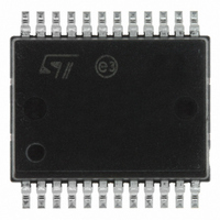
VNQ5050AK-E STMicroelectronics, VNQ5050AK-E Datasheet - Page 11

VNQ5050AK-E
Manufacturer Part Number
VNQ5050AK-E
Description
IC DRIVER HISIDE QUAD POWERSSO24
Manufacturer
STMicroelectronics
Type
High Sider
Datasheet
1.VNQ5050AK-E.pdf
(31 pages)
Specifications of VNQ5050AK-E
Input Type
Non-Inverting
Number Of Outputs
4
On-state Resistance
50 mOhm
Current - Peak Output
19A
Voltage - Supply
4.5 V ~ 36 V
Operating Temperature
-40°C ~ 150°C
Mounting Type
Surface Mount
Package / Case
PowerSSO-24
Lead Free Status / RoHS Status
Lead free / RoHS Compliant
Current - Output / Channel
-
Lead Free Status / Rohs Status
Lead free / RoHS Compliant
Available stocks
Company
Part Number
Manufacturer
Quantity
Price
Company:
Part Number:
VNQ5050AK-E
Manufacturer:
ST
Quantity:
4 660
Company:
Part Number:
VNQ5050AK-E
Manufacturer:
st
Quantity:
2 100
Part Number:
VNQ5050AK-E
Manufacturer:
ST
Quantity:
20 000
VNQ5050AK-E
Table 8.
1. Parameter guaranteed by design; it is not tested.
Table 9.
1. To ensure long term reliability under heavy overload or short circuit conditions, protection and related
Symbol
V
t
t
Δt
t
t
T
DSENSE1H
DSENSE2H
DSENSE1L
DSENSE2L
T
DEMAG
Symbol
I
I
V
I
T
DSENSE2H
SENSEH
HYST
limH
diagnostic signals must be used together with a proper software strategy. If the device is subjected to
abnormal conditions, this software must limit the duration and number of activation cycles.
limL
T
TSD
ON
RS
R
DC short circuit
current
Short circuit current
during thermal
cycling
Shutdown
temperature
Reset temperature
Thermal reset of
STATUS
Thermal hysteresis
(T
Turn-off output
voltage clamp
Output voltage drop
limitation
TSD
Analog sense output
current in over
temperature condition
Delay response time
from falling edge of
CS_DIS pin
Delay response time
from rising edge of
CS_DIS pin
Delay response time
from rising edge of
INPUT pin
Delay response time
between rising edge of
output current and
rising edge of current
sense
Delay response time
from falling edge of
INPUT pin
Current sense (8V<V
Protection
Parameter
-T
R
)
Parameter
(1)
Doc ID 13329 Rev 9
V
5 V<V
V
I
I
(see
OUT
OUT
CC
CC
=13 V
=13 V; T
=2 A; V
=0.1 A; T
CC
Figure
V
V
(see
V
(see
V
(see
V
I
I
I
V
(see
I
I
I
SENSE
OUT
OUTMAX
I
CC
SENSE
SENSE
SENSE
SENSE
CC
SENSE
SENSE
SENSE
SENSE
SENSE
Test conditions
<16V) (continued)
<36 V
= 13 V; V
=90 % of I
Figure
Figure
Figure
Figure
IN
9)
R
= 90 % of I
=10 % of I
=90 % of I
=90 % of I
=10 % of I
<4 V, 0.5 A<Iout<4 A
<4 V,
<4 V,
<4 V,
<4 V,
Test conditions
j
=0; L=6 mH
=2 A (see
<T
=-40 °C...150 °C
j
<T
4)
4)
4)
4)
SENSE
TSD
OUTMAX
0.5 A<Iout<4 A
0.5 A<Iout<4 A
0.5 A<Iout<4 A
SENSE max
SENSE max
SENSEMAX,
SENSE max
SENSE max
Figure
= 5 V
5)
T
V
RS
Min.
13.5
CC
150
135
-
-
-
-41
+ 1 T
Electrical specifications
Min.
-
-
-
-
-
-
V
RS
Typ.
CC
175
19
25
7
7
-
-46
+ 5
Typ.
100
50
80
8
5
-
V
Max.
26.5
26.5
CC
Max.
200
100
250
250
20
65
-
-
-
-
-
-
-52
Unit
11/31
Unit
mA
mV
µs
µs
µs
µs
µs
°C
°C
°C
°C
A
A
A
V


