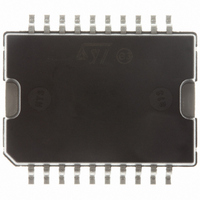
L6376D STMicroelectronics, L6376D Datasheet

L6376D
Specifications of L6376D
Available stocks
Related parts for L6376D
L6376D Summary of contents
Page 1
... This device is a monolithic quad intelligent power switch in multipower BCD technology, for driving inductive, capacitive or resistive loads. Diagnostic for CPU feedback and extensive use of electrical protections make this device inherently indistructible and suitable for general purpose industrial applications. Table 1. Order codes L6376D L6376D013TR 22nF CURRENT LIMIT ...
Page 2
Contents Contents 1 Maximum rating . . . . . . . . . . . . . . . . . . . . . . . . . . . . . . . . . . . ...
Page 3
L6376 1 Maximum rating Table 2. Absolute maximum ratings Symbol Pin out 12, 13, i 14, 15 out 9 ...
Page 4
Pin connections 2 Pin connections Figure 2. Pin connections (top view) Table 3. Pin description N# Pin name 10, GND 11, ...
Page 5
L6376 Table 3. Pin description (continued) N# Pin name 19 DIAG Function Diagnostic output. This open drain output reports the IC working condition. The bad condition (as undervoltage, overcurrent, overtemperature) turns the output low. ...
Page 6
Thermal characteristics 3 Thermal characteristics Table 4. Thermal data Symbol Thermal resistance, junction to ambient R thJA (see thermal characteristics) R Thermal resistance junction-case thJC Note: Additional data on the PowerSO-20 can be found in Application note AN668 6/18 Parameter ...
Page 7
L6376 4 Electrical characteristics Table 5. Electrical characteristcs ( Symbol Pin# DC operation sth 6 V shys I qsc 12,13, 14,15, I bias 18 V ihys Θ lim ...
Page 8
Electrical characteristics Table 5. Electrical characteristcs (continued Symbol Pin# AC operation ...
Page 9
L6376 Figure 3. Undervoltage comparator hysteresis Figure 4. Switching waveforms out V shys D94IN126A V sth 50 90% 50% 10 Electrical characteristics 90% 50% 10 ...
Page 10
Overtemperature protection (OVT) 5 Overtemperature protection (OVT) If the chip temperature exceeds Θlim (measured in a central position in the chip) the chip deactivates itself. The following actions are taken: ● all the output stages are switched off; ● the ...
Page 11
L6376 8 Short circuit operation In order to allow normal operation of the other inputs when one channel is in short cirtuit, an innovative non dissipative over current protection (patent pending) is implemented in the device. Figure 5. Short circuit ...
Page 12
Programmable diagnostic delay Typical waveforms for short circuit operation are shown in If both the ON DELAY and the OFF DELAY pins are grounded the non dissipative over current protection is inhibited and the outputs in short circuit remain on ...
Page 13
L6376 11 Demagnetization of inductive loads The device has four internal clamping diodes able to demagnetize inductive loads. The limitation is the peak power dissipation of the packages, so — if the loads are big or if there is the ...
Page 14
Demagnetization of inductive loads Figure 8. External demagnetization circuit (versus DRIVER UV SHORT CIRCUIT 14/ CURRENT OVC LIMIT CONTROL D94IN110A V S (max ...
Page 15
L6376 12 Package mechanical data In order to meet environmental requirements, ST offers these devices in ECOPACK® packages. These packages have a lead-free second level interconnect . The category of second level interconnect is marked on the package and on ...
Page 16
Package mechanical data Figure 9. Package dimensions 45˚ 16/ DETAIL PSO20MEC DETAIL B E DETAIL A lead ...
Page 17
L6376 13 Revision history Table 7. Document revision history Date September 2003 03-Mar-2008 Revision 5 First issue in EDOCS dms. 6 Modified: Removed obsolete package DIP-20 Revision history Changes 17/18 ...
Page 18
... Information in this document is provided solely in connection with ST products. STMicroelectronics NV and its subsidiaries (“ST”) reserve the right to make changes, corrections, modifications or improvements, to this document, and the products and services described herein at any time, without notice. All ST products are sold pursuant to ST’s terms and conditions of sale. ...


