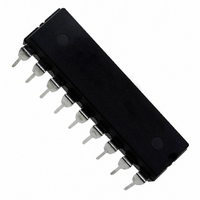
L6506 STMicroelectronics, L6506 Datasheet - Page 3

L6506
Manufacturer Part Number
L6506
Description
IC STEPPER MOTOR CTRLR 18-DIP
Manufacturer
STMicroelectronics
Type
Stepper Motor Controller/Driverr
Datasheet
1.L6506D013TR.pdf
(8 pages)
Specifications of L6506
Applications
Stepper Motor Controller
Number Of Outputs
4
Voltage - Supply
4.5 V ~ 7 V
Mounting Type
Through Hole
Package / Case
18-DIP (0.300", 7.62mm)
Product
Stepper Motor Controllers / Drivers
Operating Supply Voltage
10 V
Supply Current
25 mA
Mounting Style
Through Hole
Operating Temperature
150 C
Current, Input Bias
1 uA (Max.)
Current, Quiescent Supply
25 mA (Max.)
Frequency
5 to 70 kHz
Number Of Pins
18
Package Type
DIP18
Power Dissipation
1 W
Temperature, Junction, Maximum
150 °C
Temperature, Storage
-40 to +150 °C
Thermal Resistance, Junction To Ambient
80 °C⁄W (Max.)
Voltage, Input
-0.3 to 3 V
Voltage, Input, High Level
2 V (Min.)
Voltage, Input, Low Level
0.8 V (Max.)
Voltage, Supply
4.5 to 7 V
Lead Free Status / RoHS Status
Lead free / RoHS Compliant
Current - Output
-
Operating Temperature
-
Voltage - Load
-
Lead Free Status / Rohs Status
Lead free / RoHS Compliant
Other names
497-2945-5
Available stocks
Company
Part Number
Manufacturer
Quantity
Price
Part Number:
L6506
Manufacturer:
ST
Quantity:
20 000
Company:
Part Number:
L6506A
Manufacturer:
AMIS
Quantity:
6 219
Part Number:
L6506D
Manufacturer:
ST
Quantity:
20 000
Company:
Part Number:
L6506D013TR
Manufacturer:
STM
Quantity:
212
Part Number:
L6506D013TR
Manufacturer:
ST
Quantity:
20 000
ELECTRICAL CHARACTERISTICS (continued)
COMPARATOR SECTION PERFORMANCE (Over Operating Temperature Range)
LOGIC SECTION (Over Operating Temperature Range - TTL compatible inputs & outputs)
OSCILLATOR
CIRCUIT OPERATION
The L6506 is intended for use with dual bridge driv-
ers, such as the L298, quad darlington arrays, such
as the L7150, quad DMOS array such as L6114-
L6115, or discrete power transistors to drive stepper
motors and other similar loads. The main function of
the device is to sense and control the current in each
of the load windings.
A common on-chip oscillator drives the dual chopper
and sets the operating frequency for the pulse width
modulated drive. The RC network on pin 1 sets the
operating frequency which is given by the equation
:
The oscillator provides pulses to set the two flip-
flops which in turn cause the outputs to activate the
drive. When the current in the load winding reaches
the programmed peak value, the voltage across the
sense resistor (R
responding comparator resets its flip-flop interrupt-
ing the drive current until the next oscillator pulse oc-
curs. The peak current in each winding is pro-
grammed by selecting the value of the sense resis-
Symbol
Symbol
Symbol
V
V
V
V
V
V
f
I
V
I
osc
OH
R
IO
thH
IO
OH
thL
IH
OL
IL
i
f =
Input Offset Voltage
Input Offset Curent
Input High Voltage
Input Low Voltage
Output High Voltage
Ouptut Low Voltage
Ouput Source Current - Outputs
1 - 4
Frequency Range
Lower Threshold Voltage
Higher Threshold Voltage
Internal Discharge Resistor
0.69 RC
1
sense
Parameter
Parameter
Parameter
) is equal to V
for R
10 K
ref
and the cor-
V
V
I
V
I
V
OH
OH
IN
CC
CC
CC
= 1.4V
= 400 A
= 4mA
= 4.75V
= 4.75V
= 4.75V
Test Condtions
Test Condtions
Test Condtions
tor and V
each chopper, each of the loads may be pro-
grammed independently allowing the device to be
used to implement microstepping of the motor.
Lower threshold of L6506’s oscillator is 1/3 V
per threshold is 2/3 V
sistor is 1 K
Ground noise problems in multiple configurations
can be avoided by synchronizing the oscillators.
This may be done by connecting the sync pins of
each of the devices with the oscillator output of the
master device and connecting the R/C pin of the un-
used oscillators to ground.
The equations for the active time of the sync pulse
(T2), the inactive time of the sync signal (T1) and the
duty cycle can be found by looking at the figure 1 and
are :
ref
T2 = 0.69 C1
. Since separate inputs are provided for
T1 = 0.69 R1 C1
DC =
Min.
30 %.
0.7
5
Min.
Min.
2.75
T1 + T2
2
2
CC
T2
0.33 V
0.66 V
and internal discharge re-
R1 + R
Typ.
R1 R
1
Typ.
Typ.
0.25
3.5
L6506 - L6506D
CC
CC
IN
IN
Max.
Max.
Max.
0.8
0.4
1.3
500
70
V
20
s
CC
Unit
Unit
Unit
KHz
mV
mA
nA
k
V
V
V
V
V
V
. Up-
(1)
(2)
(3)
3/8


