L6235N STMicroelectronics, L6235N Datasheet - Page 8
L6235N
Manufacturer Part Number
L6235N
Description
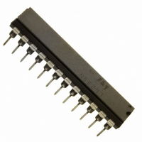
IC DRIVER 3PHASE MOTOR 24-PWRDIP
Manufacturer
STMicroelectronics
Type
Driverr
Datasheet
1.L6235D013TR.pdf
(25 pages)
Specifications of L6235N
Applications
DC Motor Driver, Brushless (BLDC), 3 Phase
Number Of Outputs
1
Current - Output
5.6A
Voltage - Supply
12 V ~ 52 V
Operating Temperature
-25°C ~ 125°C
Mounting Type
Through Hole
Package / Case
24-DIP (0.300", 7.62mm)
Operating Supply Voltage
7 V to 52 V
Supply Current
0.006 A
Mounting Style
Through Hole
Motor Type
Three Phase DC Brushless
No. Of Outputs
3
Output Current
7.1A
Output Voltage
52V
Supply Voltage Range
8V To 52V
Driver Case Style
DIP
No. Of Pins
24
Rohs Compliant
Yes
For Use With
497-4935 - BOARD MOTOR BRUSHLESS DC L6235
Lead Free Status / RoHS Status
Lead free / RoHS Compliant
Voltage - Load
-
Lead Free Status / Rohs Status
Lead free / RoHS Compliant
Other names
497-5353-5
L6235N
L6235N


L6235
CIRCUIT DESCRIPTION
POWER STAGES and CHARGE PUMP
The L6235 integrates a Three-Phase Bridge, which
consists of 6 Power MOSFETs connected as shown
on the Block Diagram. Each Power MOS has an
R
fast freewheeling diode. Switching patterns are gen-
erated by the PWM Current Controller and the Hall
Effect Sensor Decoding Logic (see relative para-
graphs). Cross conduction protection is implemented
by using a dead time (t
internal timing circuit between the turn off and turn on
of two Power MOSFETs in one leg of a bridge.
Pins VS
the supply voltage (V
Using N-Channel Power MOS for the upper transis-
tors in the bridge requires a gate drive voltage above
the power supply voltage. The Bootstrapped Supply
(V
few external components to realize a charge pump
circuit as shown in Figure 3. The oscillator output (pin
VCP) is a square wave at 600KHz (typically) with 10V
amplitude. Recommended values/part numbers for
the charge pump circuit are shown in Table1.
Table 1. Charge Pump External Component
Values.
Figure 3. Charge Pump Circuit
8/25
DS(ON)
C
C
R
D
D
BOOT
BOOT
P
P
1
2
VCP
) is obtained through an internal oscillator and
A
= 0.3
and VS
D1
R
C
P
P
D2
VBOOT
(typical value @25°C) with intrinsic
B
MUST be connected together to
S
C
).
BOOT
DT
= 1µs typical value) set by
220nF
10nF
100
1N4148
1N4148
VS
A
VS
B
D01IN1328
V
S
LOGIC INPUTS
Pins FWD/REV, BRAKE, EN, H
CMOS and µC compatible logic inputs. The internal
structure is shown in Figure 4. Typical value for turn-
ON and turn-OFF thresholds are respectively V
= 1.8V and V
Pin EN (enable) may be used to implement Overcurrent
and Thermal protection by connecting it to the open col-
lector DIAG output If the protection and an external dis-
able function are both desired, the appropriate
connection must be implemented. When the external
signal is from an open collector output, the circuit in Fig-
ure 5 can be used . For external circuits that are push
pull outputs the circuit in Figure 6 could be used. The re-
sistor R
180K . Recommended values for R
spectively 100K
lecting the values can be found in the Overcurrent
Protection section.
Figure 4. Logic Input Internal Structure
Figure 5. Pin EN Open Collector Driving
Figure 6. Pin EN Push-Pull Driving
COLLECTOR
PUSH-PULL
OUTPUT
OUTPUT
OPEN
EN
should be chosen in the range from 2.2K to
R
th(OFF)
EN
5V
C
R
EN
PROTECTION
EN
C
and 5.6nF. More information for se-
EN
= 1.3V.
ESD
DIAG
DIAG
EN
EN
PROTECTION
5V
PROTECTION
1
D01IN1329
, H
ESD
ESD
EN
2
and H
and C
5V
5V
3
EN
are TTL/
D02IN1378
D02IN1379
are re-
th(ON)
Related parts for L6235N
Image
Part Number
Description
Manufacturer
Datasheet
Request
R

Part Number:
Description:
DMOS DRIVER FOR THREE-PHASE BRUSHLESS DC MOTOR
Manufacturer:
STMicroelectronics
Datasheet:

Part Number:
Description:
EVAL BOARD FOR L6229PD SOIC
Manufacturer:
STMicroelectronics
Datasheet:
Part Number:
Description:
L6235 THREE PHASE BRUSHLESS DC MOTOR DRIVER
Manufacturer:
STMicroelectronics
Datasheet:
Part Number:
Description:
STMicroelectronics [RIPPLE-CARRY BINARY COUNTER/DIVIDERS]
Manufacturer:
STMicroelectronics
Datasheet:
Part Number:
Description:
STMicroelectronics [LIQUID-CRYSTAL DISPLAY DRIVERS]
Manufacturer:
STMicroelectronics
Datasheet:

Part Number:
Description:
BOARD EVAL FOR MEMS SENSORS
Manufacturer:
STMicroelectronics
Datasheet:
Part Number:
Description:
NPN TRANSISTOR POWER MODULE
Manufacturer:
STMicroelectronics
Datasheet:
Part Number:
Description:
TURBOSWITCH ULTRA-FAST HIGH VOLTAGE DIODE
Manufacturer:
STMicroelectronics
Datasheet:
Part Number:
Description:
Manufacturer:
STMicroelectronics
Datasheet:
Part Number:
Description:
DIODE / SCR MODULE
Manufacturer:
STMicroelectronics
Datasheet:
Part Number:
Description:
DIODE / SCR MODULE
Manufacturer:
STMicroelectronics
Datasheet:
Part Number:
Description:
Search -----> STE16N100
Manufacturer:
STMicroelectronics
Datasheet: