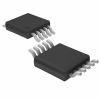
LT4351CMS Linear Technology, LT4351CMS Datasheet - Page 9

LT4351CMS
Manufacturer Part Number
LT4351CMS
Description
IC CTRLR MOSFET DIODE-OR 10MSOP
Manufacturer
Linear Technology
Datasheet
1.LT4351IMSPBF.pdf
(20 pages)
Specifications of LT4351CMS
Applications
Paralleled/Redundant Power Supplies
Fet Type
N-Channel
Number Of Outputs
1
Internal Switch(s)
No
Delay Time - Off
600ns
Voltage - Supply
1.2 V ~ 18 V
Current - Supply
1.4mA
Operating Temperature
0°C ~ 70°C
Mounting Type
Surface Mount
Package / Case
10-MSOP, Micro10™, 10-uMAX, 10-uSOP
Lead Free Status / RoHS Status
Contains lead / RoHS non-compliant
Delay Time - On
-
Available stocks
Company
Part Number
Manufacturer
Quantity
Price
Part Number:
LT4351CMS
Manufacturer:
LINEAR/凌特
Quantity:
20 000
Company:
Part Number:
LT4351CMS#PBF
Manufacturer:
SEMTECH
Quantity:
731
Part Number:
LT4351CMS#PBF
Manufacturer:
LINEAR/凌特
Quantity:
20 000
Part Number:
LT4351CMS#TRPBF
Manufacturer:
LINEAR/凌特
Quantity:
20 000
Company:
Part Number:
LT4351CMSTRPBF
Manufacturer:
LINEAR
Quantity:
2 387
APPLICATIONS INFORMATION
OPERATION
The on-chip boost regulator uses a constant off-time
control scheme. When V
voltage, the switch turns on after a 600ns off-time. When
the switch turns on current ramps up in the inductor until
the current limit is reached (450mA). The switch turns
off and the inductor’s current flows through the external
diode to charge up the V
the switch turns on again after a fixed off-time of 600ns.
Setting Fault Thresholds
The gate drive amplifier implements the ideal diode func-
tion. The fault comparators (UV and OV) prevent out of
range input voltages from affecting the output by disabling
the amplifier during these conditions. Think of the UV and
OV as gating the ideal diode function, something a regular
diode cannot do.
A resistive divider from V
are the usual way of setting the FAULT thresholds. For UV
the resistor values are set by:
where UV
the input. UV
UV TURNING ON
R2 =
R1=
V
IN
R2
R1
UV
UV
I
UV
UVHYST
HYST
FAULT
HYST
I
10µA
HYS
V
300mV
FAULT
Figure 1
V
UV
UV
is the desired undervoltage hysteresis at
– V
is the desired undervoltage trip volt-
UV TURNING OFF
UV
V
IN
R2
R1
4351 F01
DD
UV
• R2
IN
DD
capacitor. If V
to UV and one from V
is below the regulation trip
I
10µA
HYS
V
300mV
UV
DD
is still too low,
Figure 2
V
IN
IN
R
OV
R
4351 F02
B
A
to OV
V
300mV
OV
The boost regulator regulates V
above V
turn-on is disabled. When V
hysteresis level, the SW transistor is allowed to turn on.
There is approximately 0.15V of hysteresis.
age at the input. V
(0.3V) and I
(10µA). See Figure 1.
The divider on the OV pin is a straightforward resistive
divider (Figure 2):
where OV
input and V
has 7mV of voltage hysteresis at room.
It is possible to do both dividers together using only three
resistors though with more interdependence in compo-
nents (Figure 3). The input bias current for UV and OV is
less than 200nA, so keep resistor values less than 10k.
R
R
B
A
=
=
IN
R
FAULT
When V
OV
A
OV
HYSTUV
,R
V
V
FAULT
Figure 3
IN
OV
is the OV pin threshold (0.3V). The OV pin
B
R3
R2
R1
is the desired overvoltage trip point at the
4351 F03
Divider Current
DD
UV
0.3V
is the undervoltage hysteresis current
UV
OV
– 1
is above this level, the SW transistor
is the part undervoltage trip point
R
A
DD
falls below this level by the
DD
to approximately 10.7V
Figure 4
C1
V
LT4351
IN
R2B
R2A
R1
4351 F04
UV
4351fc
9


