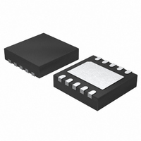
LTC4413EDD-2#TRPBF Linear Technology, LTC4413EDD-2#TRPBF Datasheet - Page 7

LTC4413EDD-2#TRPBF
Manufacturer Part Number
LTC4413EDD-2#TRPBF
Description
IC IDEAL DIODE DUAL 10-DFN
Manufacturer
Linear Technology
Datasheet
1.LTC4413EDD-1PBF.pdf
(16 pages)
Specifications of LTC4413EDD-2#TRPBF
Applications
Handheld/Mobile Devices
Fet Type
P-Channel
Number Of Outputs
2
Internal Switch(s)
Yes
Delay Time - On
11µs
Delay Time - Off
2µs
Voltage - Supply
2.5 V ~ 5.5 V
Current - Supply
40µA
Operating Temperature
-40°C ~ 85°C
Mounting Type
Surface Mount
Package / Case
10-DFN
Lead Free Status / RoHS Status
Lead free / RoHS Compliant
Available stocks
Company
Part Number
Manufacturer
Quantity
Price
PIN FUNCTIONS
INA (Pin 1): Primary Ideal Diode Anode and Positive Power
Supply for LTC4413-1/LTC4413-2. Bypass INA with a ce-
ramic capacitor of at least 1μF . (Series 1Ω snub resistors
and higher valued capacitances are recommended when
large inductances are in series with this input.) This pin
can be grounded when not used. Limit slew rate on this
pin to less than 2.5V/μs.
ENBA (Pin 2): Enable Low for Diode A. Pull this pin high
to shut down this power path. Tie to GND to enable.
Refer to Table 1 for mode control functionality. This pin
can be left fl oating, a weak (3.5μA) pull-down internal to
LTC4413-1/LTC4413-2 is included.
GND (Pin 3): Power Ground for the IC.
ENBB (Pin 4): Enable Low for Diode B. Pull this pin high
to shut down this power path. Tie to GND to enable.
Refer to Table 1 for mode control functionality. This pin
can be left fl oating, a weak (3.5μA) pull-down internal to
LTC4413-1/LTC4413-2 is included.
INB (Pin 5): Secondary Ideal Diode Anode and Positive
Power Supply for LTC4413-1/LTC4413-2. Bypass INB with a
ceramic capacitor of at least 1μF . (Series 1Ω snub resistors
and higher valued capacitances are recommended when
large inductances are in series with this input.) This pin
can be grounded when not used. Limit slew rate on this
pin to less than 2.5V/μs.
OUTB (Pin 6): Secondary Ideal Diode Cathode and Output
of the LTC4413-1/LTC4413-2. Bypass OUTB with a high
(1mΩ min) ESR ceramic capacitor of at least 4.7μF . This
pin must be left fl oating when not in use. Limit slew rate
on this pin to less than 2.5V/μs.
OVP (Pin 7, LTC4413-2 Only): Drive Output for an Exter-
nal OVP Switch PMOS Transistor (To Inhibit Overvoltage
Wall Adapter Voltages from Damaging Device.) During
overvoltage conditions, this output will remain high so
long as an overvoltage condition persists. This pin must
be left fl oating when not in use.
OVI (Pin 8, LTC4413-2 Only): Sense Input for Overvoltage
Protection Block. This pin can be left fl oating or grounded
when not used.
STAT (Pin 9): Status Condition Indicator. Weak (11μA)
pull-down current output. When terminated, high indicates
diode conducting. Refer to Table 2 for the operation of this
pin. This pin can also be left fl oating or grounded.
OUTA (Pin 10): Primary Ideal Diode Cathode and Output
of the LTC4413-1/LTC4413-2. Bypass OUTA with a high
(1mΩ min) ESR ceramic capacitor of at least 4.7μF . This
pin must be left fl oating when not in use. Limit slew rate
on this pin to less than 2.5V/μs.
Exposed Pad (Pin 11): Signal Ground. This pin must be
soldered to PCB ground to provide both electrical contact
to ground and good thermal contact to PCB.
LTC4413-1/LTC4413-2
441312fd
7


