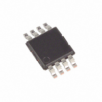
MAX8535EUA+T Maxim Integrated Products, MAX8535EUA+T Datasheet - Page 14

MAX8535EUA+T
Manufacturer Part Number
MAX8535EUA+T
Description
IC CNTRLR ORING MOSFET 8-MSOP
Manufacturer
Maxim Integrated Products
Datasheet
1.MAX8535EUA.pdf
(20 pages)
Specifications of MAX8535EUA+T
Applications
Network/Telecom Power Supplies, Rectifiers
Fet Type
N-Channel
Number Of Outputs
1
Internal Switch(s)
No
Delay Time - Off
200ns
Voltage - Supply
8 V ~ 14 V
Current - Supply
2mA
Operating Temperature
-40°C ~ 85°C
Mounting Type
Surface Mount
Package / Case
8-MSOP, Micro8™, 8-uMAX, 8-uSOP,
Lead Free Status / RoHS Status
Lead free / RoHS Compliant
Delay Time - On
-
Lead Free Status / Rohs Status
Lead free / RoHS Compliant
ORing MOSFET Controllers with Fastest
Fault Isolation for Redundant Power Supplies
Normally, the external MOSFET’s gate capacitance is
sufficient to serve as a reservoir capacitor. If the
MOSFETs are located at a significant distance from the
MAX8535/MAX8536/MAX8585, place a local bypass
capacitor (0.01µF, typ) across GATE and GND. For
slower turn-on times, add a small capacitor between
GATE and GND and a series resistor between GATE
and the gate of the MOSFETs.
To set the undervoltage lockout threshold, use a resistor-
divider connected between V
center node of the divider connected to UVP. For
example, use a 10k
to GND and calculate the other resistor (R3) using:
where V
age and V
in the Electrical Characteristics (1.25V, typ). To defeat
the UVP, leave UVP unconnected.
To set the OVP threshold, use a resistor-divider con-
nected between CS and GND, with the center node of
the divider connected to OVP. For example, use a
10k
calculate the other resistor, R5, using:
where V
and V
the Electrical Characteristics (1.25V, typ). To defeat the
OVP, connect the OVP input to GND.
The MAX8535/MAX8536/MAX8585 drive n-channel
MOSFETs. The most important feature of the MOSFETs
is R
MOSFET, a voltage (V
source due to the MOSFET’s on-resistance, R
The MAX8535/MAX8536/MAX8585 monitor V
14
DS(ON)
______________________________________________________________________________________
OVP
resistor (R6 in Figure 4) from OVP to GND and
OVLO
UVLO
UVP
. As load current flows through the external
is the OVP reference threshold specified in
is the desired overvoltage lockout voltage
is the desired undervoltage lockout volt-
is the UVP reference threshold specified
R
R
3
5
Set the UVP Fault Threshold
Set the OVP Fault Threshold
resistor (R4 in Figure 4) from UVP
R
R
DS
4
6
) is generated from drain-to-
V
V
V
V
UVLO
OVLO
UVP
OVP
CC
MOSFET Selection
-
-
and GND, with the
1
1
DS
DS(ON)
of the
.
MOSFETs at all times. The MAX8535/MAX8536/
MAX8585 determine the state of the monitored power
supply by measuring the voltage drop across the exter-
nal MOSFETs. With two external MOSFETs, the equa-
tion becomes:
Selecting a MOSFET with a low R
current to flow through the MOSFETs before the
MAX8535/MAX8536/MAX8585 detect reverse-current
(I
Single MOSFETs can be used if the OVP function is not
needed. Connect the source of the MOSFET to V
and the drain of the MOSFET to CS.
Keep all traces as short as possible and maximize the
high-current trace width to reduce the effect of undesir-
able parasitic inductance. The MOSFET generates a
fair amount of heat because of the high currents
involved. In order to dissipate the heat generated by
the MOSFET, make the power traces very wide with a
large amount of copper area, and place the MAX8535/
MAX8536/MAX8585 as close as possible to the drain of
the external MOSFET. A more efficient way to achieve
good power dissipation on a surface-mount package is
to lay out two copper pads directly under the MOSFET
package on both sides of the board. Connect the two
pads to the ground plane through vias and use
enlarged copper mounting pads on the topside of the
board. Use a ground plane to minimize impedance and
inductance. Refer to the MAX8535 Evaluation Kit data
sheet for an example of a PC board layout.
In addition to the usual high-power considerations,
bypassing prevent false faults by:
REVERSE
1) Bypass V
2) Making the traces connecting UVP and OVP as
3) Kelvin connecting V
V
DSTOTAL
bypassing CS with a 1nF capacitor to ground.
short as possible.
MOSFET.
) and forward-current (I
= R
CC
DS(ON)1
with a 0.1µF capacitor to ground and
x I
Using a Single MOSFET
CC
LOAD
and CS to the external
Layout Guidelines
FORWARD
+ R
DS(ON)
DS(ON)2
) conditions.
allows more
x I
LOAD
CC


