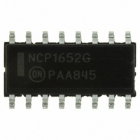
NCP1652DR2G ON Semiconductor, NCP1652DR2G Datasheet - Page 28

NCP1652DR2G
Manufacturer Part Number
NCP1652DR2G
Description
IC PFC CONTROLLER CCM/DCM 16SOIC
Manufacturer
ON Semiconductor
Datasheet
1.NCP1652DR2G.pdf
(34 pages)
Specifications of NCP1652DR2G
Mode
Continuous Conduction (CCM), Discontinuous Conduction (DCM)
Frequency - Switching
100kHz
Current - Startup
5.62mA
Voltage - Supply
9.3 V ~ 20 V
Operating Temperature
-40°C ~ 125°C
Mounting Type
Surface Mount
Package / Case
16-SOIC (3.9mm Width)
Switching Frequency
20 KHz to 250 KHz
Maximum Operating Temperature
+ 125 C
Mounting Style
SMD/SMT
Minimum Operating Temperature
- 40 C
Lead Free Status / RoHS Status
Lead free / RoHS Compliant
Other names
NCP1652DR2GOSTR
converter. There is no error in the output signal due to the
series rectifier as shown in Figure 67.
is applied to the AC_IN pin by means of a resistive voltage
divider. The multiplier ramp is generated by comparing the
scaled line voltage to the oscillator ramp with the AC_IN
Comparator. The current signal from the V-I converter is
The V
voltage. A resistive voltage divider attenuates the full wave
rectified line voltage between 0.7 and 5.0 V. The full wave
rectified line is then averaged with a capacitor. The ac
average voltage must be constant over each half cycle of the
line. Line voltage ripple (120 Hz or 100 Hz) ripple on the
V
will distort the ac reference signal and reduce the power
factor and increase the line current distortion. Excessive
filtering delays the feedforward signal reducing the line
transient response. A good starting point is to set the filter
time constant to one cycle of the line voltage. The user can
then optimize the filter for line transient response versus
power factor. The average voltage on the V
Where, a is the voltage divider ratio, normally 0.01.
FF
The scaled version of the full wave rectified input ac wave
The third input to the reference generator is the V
signal adds ripple to the output of the multiplier. This
FF
AC IN
CM
V
FB
FF
signal is a dc voltage proportional to the ac line
V
FF
Multiplier
+
2
p
Oscillator
+
−
Vac 2a
Square
V−to−I
FF
Figure 67. Reference Generator
pin is:
FF
(eq. 7)
http://onsemi.com
signal.
V
FF
2
28
factored by the AC_IN comparator output. The resulting
signal is filtered by the low pass R-C filter on the CM pin.
The low pass filter removes the high frequency content. The
gain of the multiplier is determined by the V-I converter, the
resistor on the CM pin, and the peak and valley voltages of
the oscillator sawtooth ramp.
The output of the multiplier is the AC_REF. It connects to
the AC Error Amplifier.
where, k is the reference generator gain, typically 0.55. The
output of the reference generator is clamped at 4.5 V to limit
the maximum output power.
independent of the line voltage. That is, for a given FB
voltage, if the line voltage doubles (AC_IN), the
feedforward term quadruples and reduces the output of the
error amplifier in half to maintain the same input power.
AC Error Amplifier Compensation
of R
(EA). The value of the compensation components is
Divide
The multiplier transfer function is given by Equation 8.
Feedforward maintains a constant input power
A pole-zero pair is created by placing a series combination
COMP
V
AC_REF
and C
+ k @
V
COMP
AC_REF
V
FB
V
@ V
FF
at the output of the AC error amplifier
AC_IN
2
+
V
FB
V
@ V
FF
AC_IN
2
@ k
AC_REF
(eq. 8)


