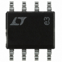
LT1249IS8 Linear Technology, LT1249IS8 Datasheet - Page 6

LT1249IS8
Manufacturer Part Number
LT1249IS8
Description
IC PFC CTRLR AVERAGE CURR 8SOIC
Manufacturer
Linear Technology
Datasheet
1.LT1249CN8PBF.pdf
(12 pages)
Specifications of LT1249IS8
Mode
Average Current
Frequency - Switching
100kHz
Current - Startup
250µA
Voltage - Supply
15.5 V ~ 27 V
Operating Temperature
-40°C ~ 125°C
Mounting Type
Surface Mount
Package / Case
8-SOIC (3.9mm Width)
Lead Free Status / RoHS Status
Contains lead / RoHS non-compliant
Available stocks
Company
Part Number
Manufacturer
Quantity
Price
Part Number:
LT1249IS8
Manufacturer:
LINEAR/凌特
Quantity:
20 000
Part Number:
LT1249IS8#PBF
Manufacturer:
LINEAR/凌特
Quantity:
20 000
Part Number:
LT1249IS8#TRPBF
Manufacturer:
LINEAR/凌特
Quantity:
20 000
PIN
APPLICATIONS
LT1249
V
amplifier.
V
a very fast gate driver required to fast charge high power
MOSFET gate capacitance. High current spikes occur
during charging. For good supply bypass, a 0.1 F ceramic
Error Amplifier
The error amplifier has a 100dB DC gain and 1.5MHz unity-
gain frequency. It is internally clamped at 12V. The nonin-
verting input is tied to the 7.5V reference.
Current Amplifier
The multiplier output current I
through the 4k resistor R
signal to the current loop that is controlled by the current
amplifier. Current gain is the ratio of R
sense resistor. The current amplifier is a transconductance
amplifier. Typical g
load. The inverting input is internally tied to GND. The
noninverting input is tied to the multiplier output. The
output is internally clamped at 8V. Output resistance is
about 4M; DC loading should be avoided because it will
lower the gain and introduce offset voltage at the inputs
which becomes a false reference signal to the current loop
and can distort line current. Note that in the current
averaging operation, high gain at twice the line frequency
is necessary to minimize line current distortion. Because
CA
condition, 11mV will be present at the inputs of the current
amplifier if gain is rolled off to 450 at 120Hz (1nF in series
with 10k at CA
less than 100mV, lower gain will distort the current loop
reference signal and line current. If signal gain at the
100kHz switching frequency is too high, the system
behaves more like a current mode system and can cause
subharmonic oscillation. Therefore, the current amplifier
should be compensated to have a gain of less than 15 at
100kHz and more than 300 at 120Hz.
6
SENSE
CC
OUT
U
(Pin 7): This is the supply of the chip. The LT1249 has
FUNCTIONS
may need to swing 5V over one line cycle at high line
(Pin 6): This is the inverting input to the voltage
U
OUT
). At light load, when (I
m
U
is 320 mho and gain is 60dB with no
U
MOUT
INFORMATION
U
M
and develops the reference
flows out of the M
W
MOUT
M
)(R
to line current
MOUT
U
) can be
OUT
pin
capacitor in parallel with a low ESR electrolytic capacitor,
56 F or higher is required in close proximity to IC GND.
GTDR (Pin 8): The MOSFET gate driver is a 1.5A fast totem
pole output. It is clamped at 15V. Capacitive loads like
MOSFET gates may cause overshoot. A gate series resis-
tor of at least 5 will prevent the overshoot.
Multiplier
The multiplier is a current multiplier with high noise
immunity in a high power switching environment. The
current gain is:
With a square function, because of the lower gain at light
power load, system stability is maintained and line current
distortion caused by the AC ripple fed back to the error
amplifier is minimized. Note that switching ripple on the
high impedance lines could get into the multiplier from the
I
internal 25k resistor in series with the low impedance
multiplier current input so that only a capacitor from the
I
multiplier output current is limited to 250 A. Figure 1
shows the multiplier transfer curves.
AC
AC
I
I
M
EA
pin to GND is needed to filter out the noise. Maximum
pin and cause instability. The LT1249 provides an
= (I
= (VA
Figure 1. Multiplier Current I
AC
300
150
)(I
OUT
0
0
EA
2
– 1.5V)/25k
VA
)/(200 A)
OUT
VA
VA
= 5.5V
OUT
OUT
= 6V
= 6.5V
I
AC
2
, and
250
( A)
M
vs I
AC
and VA
1249 G04
500
VA
VA
VA
VA
VA
VA
VA
OUT
OUT
OUT
OUT
OUT
OUT
OUT
OUT
= 5V
= 4.5V
= 4V
= 3.5V
= 3V
= 2.5V
= 2V


