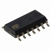
L6563A STMicroelectronics, L6563A Datasheet - Page 5

L6563A
Manufacturer Part Number
L6563A
Description
IC PFC CTRLR TRANSITION 14SOIC
Manufacturer
STMicroelectronics
Datasheet
1.L6563ATR.pdf
(39 pages)
Specifications of L6563A
Mode
Discontinuous (Transition)
Current - Startup
50µA
Voltage - Supply
10.3 V ~ 22 V
Operating Temperature
-25°C ~ 125°C
Mounting Type
Surface Mount
Package / Case
14-SOIC (3.9mm Width), 14-SOL
Maximum Operating Temperature
+ 150 C
Mounting Style
SMD/SMT
Minimum Operating Temperature
- 25 C
For Use With
497-9082 - EVAL BOARD L6563 (200W)497-8850 - BOARD EVAL FOR L6563/STW55NM60N497-8834 - BOARD DEMO FOR L6563/LL6566A497-8429 - BOARD ADAPTER L6599/STP12NM50N497-5854 - DEMO BOARD FOR L6563497-5496 - EVAL BOARD FOR L6599497-5493 - EVAL BOARD FOR L6563
Lead Free Status / RoHS Status
Lead free / RoHS Compliant
Frequency - Switching
-
Lead Free Status / Rohs Status
Lead free / RoHS Compliant
Available stocks
Company
Part Number
Manufacturer
Quantity
Price
Part Number:
L6563A
Manufacturer:
ST
Quantity:
20 000
Part Number:
L6563AD013TR
Manufacturer:
ST
Quantity:
20 000
L6563 - L6563A
Table 2. Pin description (continued)
Pin N°
10
11
12
13
14
6
7
8
9
PWM_LATCH
PWM_STOP
PFC_OK
Name
GND
TBO
RUN
ZCD
VCC
GD
Tracking Boost function. This pin provides a buffered VFF voltage. A resistor connected
between this pin and GND defines a current that is sunk from pin INV (pin 1). In this way,
the output voltage is changed proportionally to the mains voltage (tracking boost). If this
function is not used leave this pin open.
PFC pre-regulator output voltage monitoring/disable function. This pin senses the output
voltage of the PFC pre-regulator through a resistor divider and is used for protection
purposes. If the voltage at the pin exceeds 2.5V the IC is shut down, its consumption goes
almost to the start-up level and this condition is latched. PWM_LATCH pin is asserted high.
Normal operation can be resumed only by cycling the Vcc. This function is used for
protection in case the feedback loop fails.
If the voltage on this pin is brought below 0.2V the IC is shut down and its consumption is
considerably reduced. To restart the IC the voltage on the pin must go above 0.26V. If these
functions are not needed, tie the pin to a voltage between 0.26 and 2.5 V.
Output pin for fault signaling. During normal operation this pin features high impedance. If
either a voltage above 2.5V at PFC_OK (pin 7) or a voltage above 1.7V on CS (pin 4) of
L6563 is detected the pin is asserted high. Normally, this pin is used to stop the operation
of the DC-DC converter supplied by the PFC pre-regulator by invoking a latched disable of
its PWM controller. If not used, the pin will be left floating.
Output pin for fault signaling. During normal operation this pin features high impedance. If
the IC is disabled by a voltage below 0.5V on RUN (pin 10) the voltage at the pin is pulled
to ground. Normally, this pin is used to temporarily stop the operation of the DC-DC
converter supplied by the PFC pre-regulator by disabling its PWM controller. If not used,
the pin will be left floating.
Remote ON/OFF control. A voltage below 0.52V shuts down (not latched) the IC and
brings its consumption to a considerably lower level. PWM_STOP is asserted low. The IC
restarts as the voltage at the pin goes above 0.6V. Connect this pin to VFF (pin 5) either
directly or through a resistor divider to use this function as brownout (AC mains
undervoltage) protection, tie to INV (pin 1) if the function is not used.
Boost inductor’s demagnetization sensing input for transition-mode operation. A negative-
going edge triggers MOSFET’s turn-on.
Ground. Current return for both the signal part of the IC and the gate driver.
Gate driver output. The totem pole output stage is able to drive power MOSFET’s and
IGBT’s with a peak current of 600 mA source and 800 mA sink. The high-level voltage of
this pin is clamped at about 12V to avoid excessive gate voltages.
Supply Voltage of both the signal part of the IC and the gate driver.
Description
Description
5/39


