FDC6331L Fairchild Semiconductor, FDC6331L Datasheet
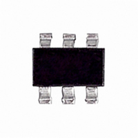
IC LOAD SWITCH INT 8VIN SSOT-6

FDC6331L

Manufacturer Part Number
FDC6331L
Description
IC LOAD SWITCH INT 8VIN SSOT-6
Manufacturer
Fairchild Semiconductor
Type
High Side Switchr
Datasheet

Specifications of FDC6331L

Number Of Outputs
1
Rds (on)
55 mOhm
Internal Switch(s)
Yes
Current Limit
2.8A
Voltage - Input
2.5 ~ 8 V
Operating Temperature
-55°C ~ 150°C
Mounting Type
Surface Mount
Package / Case
6-SSOT, SuperSOT-6
Power Switch Family
FDC6331L
Input Voltage
2.5 to 8V
Power Switch On Resistance
3.8Ohm
Output Current
2.8A
Mounting
Surface Mount
Package Type
SuperSOT
Operating Temperature (min)
-55C
Operating Temperature (max)
150C
Operating Temperature Classification
Military
Pin Count
6
Power Dissipation
700W
On Resistance (max)
3.8 Ohms
Maximum Operating Temperature
+ 150 C
Minimum Operating Temperature
- 55 C
Maximum Power Dissipation
700 mW
Mounting Style
SMD/SMT
Switch Configuration
Dual
Lead Free Status / RoHS Status
Lead free / RoHS Compliant
Other names
FDC6331L
FDC6331LTR

Available stocks

Company
Part Number
Manufacturer
Quantity
Price
Part Number:
FDC6331L
Manufacturer:
FAIRCHILD/仙童
Quantity:
20 000
Company:
Part Number:
FDC6331L
Quantity:
18 000
Company:
Part Number:
FDC6331L
Quantity:
4 500
Part Number:
FDC6331L-NL
Manufacturer:
FSC可看货
Quantity:
20 000
FDC6331L
Integrated Load Switch
General Description
This device is particularly suited for compact power
management in portable electronic equipment where
2.5V to 8V input and 2.8A output current capability are
needed. This load switch integrates a small N-Channel
power MOSFET (Q1) that drives a large P -Channel
power MOSFET (Q2) in one tiny SuperSOT
package.
Applications
2007 Fairchild Semiconductor Corporation
Absolute Maximum Ratings
Symbol
V
V
I
P
T
Thermal Characteristics
R
R
Package Marking and Ordering Information
Load
Load switch
Power management
D
J
IN
ON/OFF
SuperSOT
, T
JA
J C
Device Marking
STG
Pin 1
SuperSOT™-6
D1
.331
S1
TM
Maximum Input Voltage
High level ON/OFF voltage range
Load Current
Maximum Power Dissipation
Operating and Storage Junction Temperature Range
Thermal Resistance, Junction-to-Ambient
Thermal Resistance, Junction-to-Case
-6
D2
G1
S2
G2
– Continuous
– Pulsed
FDC6331L
Device
Parameter
ON/OFF
Vin,R1
R1,C1
T
A
4
5
6
=25
T M
o
See Application Circuit
C unless otherwise noted
-6
Reel Size
Q2
7’’
(Note 1)
(Note 1)
(Note 1)
(Note 1)
Q1
Features
–2.8 A, –8 V. R
Control MOSFET (Q1) includes Zener protection for
ESD ruggedness (>6KV Human body model)
High performance trench technology for extremely
low R
3
2
1
Vout,C1
Vout,C1
R2
DS(ON)
Tape width
R
R
DS(ON)
DS(ON)
DS(ON)
–55 to +150
8mm
Ratings
–0.5 to 8
IN
ON/OFF
180
2.8
0.7
60
= 55 m @ V
= 70 m @ V
= 100 m @ V
9
Equivalent Circuit
8
+
V
DROP
August 2001
GS
GS
April 2007
GS
= –4.5 V
= –2.5 V
FDC6331L Rev D
3000 units
= –1.8 V
Quantity
OUT
Units
C/W
C/W
W
V
V
C
A
tm

Related parts for FDC6331L

FDC6331L Summary of contents

Page 1

... Reel Size 7’’ August 2001 April 2007 –4.5 V DS(ON –2.5 V DS(ON 100 –1.8 V DS(ON) GS Equivalent Circuit IN OUT + – V DROP ON/OFF Ratings Units 8 V –0 2 0.7 W –55 to +150 C 180 C/W 60 C/W Tape width Quantity 8mm 3000 units FDC6331L Rev D ...

Page 2

... J A surface of the drain pins guar anteed by design while Pulse Test: Pulse Width < 300μs, Duty Cycle < 2.0%. FDC6331L Load Switch Application Circuit ON/OFF ...

Page 3

... Figure 2. Conduction Voltage Drop Variation with Load Current. 0.15 0.125 0.1 C 0.075 O 0. 0.025 Figure 4. On-Resistance Variation 0 125 ( 1.5V - 300us < 125 GATE TO SOURCE VOLTAGE (V) GS With Input Voltage R ( 156 °C/W JA P(pk ( Duty Cycle 100 1000 FDC6331L Rev D ...

Page 4

... TRADEMARKS The following are registered and unregistered trademarks Fairchild Semiconductor owns or is authorized to use and is not intended exhaustive list of all such trademarks. ® ACEx Across the board. Around the world™ ActiveArray™ Bottomless™ Build it Now™ CoolFET™ CROSSVOLT™ ...

Related keywords