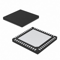
MAX8662ETM+ Maxim Integrated Products, MAX8662ETM+ Datasheet - Page 19

MAX8662ETM+
Manufacturer Part Number
MAX8662ETM+
Description
IC POWER MANAGE 48-TQFN-EP
Manufacturer
Maxim Integrated Products
Datasheet
1.MAX8662ETM.pdf
(34 pages)
Specifications of MAX8662ETM+
Applications
Handheld/Mobile Devices
Current - Supply
900µA
Voltage - Supply
4.1 V ~ 8 V
Operating Temperature
-40°C ~ 85°C
Mounting Type
Surface Mount
Package / Case
48-TQFN Exposed Pad
Lead Free Status / RoHS Status
Lead free / RoHS Compliant
MAX8662
19
20
21
22
23
24
25
26
27
28
29
30
31
32
33
34
35
36
37
38
39
PIN
MAX8663
Single-Cell, Li+ Battery-Operated Devices
16
17
18
19
20
21
22
23
24
25
—
—
—
26
27
28
29
30
31
32
—
______________________________________________________________________________________
NAME
OUT5
PWM
OVP
CC3
PG2
EN2
EN6
EN7
IN45
FB2
PV2
LX2
LX3
EN4
EN5
EN1
PG1
FB1
PV1
LX1
CS
Input Supply for Linear Regulators 4 and 5. Connect IN45 to a supply voltage between 1.7V
and V
Linear Regulator 5 Output. Delivers up to 150mA at an output voltage determined by SL1
and SL2. Connect a 1μF ceramic capacitor from OUT5 to GND. Increase the value to 2.2μF
if V
Enable Input for Linear Regulator 4. Drive high to enable.
Enable Input for Linear Regulator 5. Drive high to enable.
PWM/Skip-Mode Selector. Drive PWM high to force step-down regulators 1 and 2 to
operate in 1MHz forced-PWM mode. Drive PWM low, or connect to GND to allow regulators
1 and 2 to enter skip mode at light loads.
Feedback Input for Buck Regulator 1. Connect FB1 to the center of a resistor-divider
connected between OUT1 and GND to set the output voltage between 0.98V and 3.3V.
Enable Input for Buck Regulator 1. Drive high to enable.
Power Ground for Buck Regulator 1. GND, PG1, PG2, and PG3 must be connected
together externally.
Buck Regulator 1 Inductor Connection Node. Connect an inductor from LX1 to the output of
regulator 1.
P ow er Inp ut for Buck Reg ul ator 1. C onnect P V 1 to S Y S and d ecoup l e w i th a 10μF or g r eater l ow -
E S R cap aci tor to GN D . P V 1, P V 2, and S Y S m ust b e connected tog ether exter nal l y.
LED Boost Overvoltage Input. Connect a resistor from OVP to the boost output to set the
maximum output voltage and to initiate soft-start when EN3 goes high. An internal 20μA
pulldown current from OVP to GND determines the maximum boost voltage. The internal
current is disconnected when EN3 is low. OVP is diode clamped to SYS_.
LED Current Source. Sinks from 1mA to 30mA depending on the voltage at BRT and the
PWM signal at EN3. Driving EN3 low for more than 2ms turns off the current source. V
regulated to 0.32V.
C om p ensati on Inp ut for LE D Boost Regul ator 3. S ee the Boost C onverter w i th Whi te LE D D r i ver
( OU T3, M AX 8662 Onl y) secti on.
Feedback Input for Buck Regulator 2. Connect FB2 to the center of a resistor-divider
connected between OUT2 and GND to set the output voltage between 0.98V and 3.3V.
Power Input for Buck Regulator 2. Connect PV2 to SYS and decouple with a 10μF or
greater low-ESR capacitor to GND. PV1, PV2, and SYS must be connected together
externally.
Buck Regulator 2 Inductor Connection Node. Connect an inductor from LX2 to the output of
regulator 2.
P ower Gr ound for Buck Reg ulator 2. GN D , P G1, P G2, and PG3 must b e connected together
exter nal l y.
Enable Input for Buck Regulator 2. Drive high to enable.
Enable Input for Linear Regulator 6. Drive high to enable.
Enable Input for Linear Regulator 7. Drive high to enable.
Boost Regulator 3 Inductor Connection Node. Connect an inductor from LX3 to SYS_.
OUT5
SYS
< 1.5V.
. Connect at least a 1μF ceramic capacitor from IN45 to GND.
Power-Management ICs for
FUNCTION
Pin Description (continued)
CS
is
19


