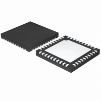
MAX8784ETL+ Maxim Integrated Products, MAX8784ETL+ Datasheet - Page 3

MAX8784ETL+
Manufacturer Part Number
MAX8784ETL+
Description
IC REG STP UP W/AMP 40-TQFN
Manufacturer
Maxim Integrated Products
Datasheet
1.MAX8784ETL.pdf
(24 pages)
Specifications of MAX8784ETL+
Applications
LCD TV/Monitor
Voltage - Supply
4 V ~ 5.5 V
Operating Temperature
-40°C ~ 85°C
Mounting Type
Surface Mount
Package / Case
40-TQFN Exposed Pad
Operating Supply Voltage
4 V to 5.5 V
Maximum Operating Temperature
- 40 C
Mounting Style
SMD/SMT
Maximum Power Dissipation
2857 mW
Minimum Operating Temperature
+ 85 C
Supply Current
4 mA
Lead Free Status / RoHS Status
Lead free / RoHS Compliant
Current - Supply
-
Lead Free Status / Rohs Status
Lead free / RoHS Compliant
ELECTRICAL CHARACTERISTICS (continued)
(V
Step-Up Regulator, Internal Charge Pumps, Switch
FB Transconductance
LX Current Limit
LX On-Resistance
Current-Sense Transresistance
Soft-Start Period
POSITIVE CHARGE-PUMP REGULATOR
V
V
FBP Regulation Voltage
FBP Line Regulation Error
FBP Input Bias Current
POUT Output-Voltage Range
POUT Fixed Output Voltage
POUT Output Current Limit
C1N, C2N High-Side On-Resistance
C1N, C2N Low-Side On-Resistance
C1P Switch On-Resistance
C2P Switch On-Resistance
POUT Switch On-Resistance
FBP Fault-Trip Level
Positive Charge-Pump Soft-Start Period 7-bit voltage ramp
NEGATIVE CHARGE-PUMP REGULATOR
FBN Regulation Voltage
FBN Input Bias Current
FBN Line Regulation Error
DRVN PCH On-Resistance
DRVN NCH On-Resistance
FBN Fault-Trip Level
N eg ati ve C har g e- P um p S oft- S tar t P er i od 7-bit voltage ramp
POSITIVE GATE-DRIVER TIMING AND CONTROL SWITCHES
CTL Input-Low Voltage
CTL Input-High Voltage
CTL Input Current
CTL-to-GON Rising Propagation Delay
CTL-to-GON Falling Propagation Delay
GON-to-POUT Switch On-Resistance
GO N - to- P OU T S w i tch S atur ati on C ur r ent
GON-to-DRN Switch On-Resistance
GON-to-DRN Switch Saturation Current V
GON-to-PGND Switch On-Resistance
CC
SUP
SUP
= +5V, Circuit of Figure 1, AVDD = SUP = +14V, T
Input Supply Range
O ver vol tag e C har g e- P um p Inhi b i t
Control, and Operational Amplifier for TFT LCDs
PARAMETER
_______________________________________________________________________________________
∆I
V
I
7-bit current ramp
V
V
V
I
HVS = V
Not in dropout, V
Falling edge
V
V
V
Rising edge
CTL = 0V or V
V
V
V
V
LX
VGON
FB
SUP
SUP
FBP
REF
FBN
SUP
GDEL
POUT
GDEL
GON
GDEL
COMP
= 1.0A
= 1.1V, duty cycle = 75%
= 1.5V
- V
= 250mV
= rising, typical hysteresis = 200mV
= 10V ~ 19V, V
= 11V to 19V, VGOFF = -9V, I
- V
= 0mA
= 1.5V, CTL = V
- V
= 1.5V, CTL = 0V
= 1.0V
FBN
= ±2.5µA, FB = COMP
CC
DRN
GON
, I
POUT
A
> 5V
CC
> 5V
= 0°C to +85°C. Typical values are at T
SUP
= 0mA
CONDITIONS
POUT
= 9V, V
CC
= 28V
POUT
= 24V
VGOFF
= -20mA
A
1.225
0.985
MIN
0.10
-100
29.1
0.96
180
-50
3.5
1.8
75
20
20
35
= +25°C, unless otherwise noted.)
-1
6
TYP
0.10
0.20
1.25
1.00
1.00
160
450
200
200
100
4.0
0.1
0.1
21
30
50
10
3
3
3
1.275
1.015
+100
MAX
0.19
0.26
30.9
15.0
10.0
10.0
1.04
280
+50
4.6
9.0
6.0
0.8
+1
19
22
36
10
20
60
6
UNITS
%/V
%/V
V/A
mA
mV
mA
mA
ms
ms
ms
kΩ
µS
nA
nA
µA
ns
ns
Ω
Ω
Ω
Ω
Ω
Ω
Ω
Ω
Ω
Ω
A
V
V
V
V
V
V
V
V
V
3


