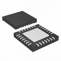
MAX8819AETI+ Maxim Integrated Products, MAX8819AETI+ Datasheet - Page 29

MAX8819AETI+
Manufacturer Part Number
MAX8819AETI+
Description
IC PMIC W/INT CHARGER 28TQFN-EP
Manufacturer
Maxim Integrated Products
Datasheet
1.MAX8819CETIT.pdf
(29 pages)
Specifications of MAX8819AETI+
Applications
Handheld/Mobile Devices
Voltage - Supply
4.1 V ~ 5.5 V
Operating Temperature
-40°C ~ 85°C
Mounting Type
Surface Mount
Package / Case
28-TQFN Exposed Pad
Mounting Style
SMD/SMT
Duty Cycle (max)
100 %
Input Voltage
4.1 V to 5.5 V
Maximum Operating Temperature
+ 85 C
Minimum Operating Temperature
- 40 C
Output Current
400 mA
Supply Current
1.33 mA
Lead Free Status / RoHS Status
Lead free / RoHS Compliant
Current - Supply
-
Lead Free Status / Rohs Status
Lead free / RoHS Compliant
constant is R x C = 100μs, and the output voltage
decays to within 1% of final value in about 500μs.
Good printed circuit board (PCB) layout is necessary to
achieve optimal performance. Refer to the MAX8819A
Evaluation Kit for Maxim’s recommended layout.
Use the following guidelines for the best results:
• The LX_ rapidly switches between PV_ and PG_.
• Keep the FB_ node away from noise sources such
• The exposed pad (EP) is the main path for heat to
• Use short and wide traces for high-current and dis-
• The step-down converter power inputs are critical
• Minimize the area of the loops formed by the step-
The top of the MAX8819_ package is laser etched as
shown in Figure 11:
“8819_ETI” is the product identification code. The full
part number is MAX8819_ETI; however, in this case, the
“MAX” prefix is omitted due to space limitations. The “_”
corresponds to the “A” or “B” version.
“yww” is a date code. “y” is the last number in the
Gregorian calendar year. “ww” is the week number in
the Gregorian calendar. For example:
• “801” is the first week of 2008; the week of
• “052” is the fifty-second week of 2010; the week of
• “aaaa” is an assembly code and lot code.
• “+” denotes lead-free packaging and marks the
Maxim cannot assume responsibility for use of any circuitry other than circuitry entirely embodied in a Maxim product. No circuit patent licenses are
implied. Maxim reserves the right to change the circuitry and specifications without notice at any time.
Maxim Integrated Products, 120 San Gabriel Drive, Sunnyvale, CA 94086 408-737-7600 ____________________ 29
© 2009 Maxim Integrated Products
Minimize stray capacitance on LX_ to maintain high
efficiency.
as the inductor.
exit the IC. Connect EP to the ground plane with
thermal vias to allow heat to dissipate from the
device.
continuous current paths.
discontinuous current paths that require careful
bypassing. Place the step-down converter input
bypass capacitor as close as possible to the PV_
and PG_ pins.
down converters’ dynamic switching currents.
January 1st, 2008.
December 27th, 2010.
pin 1 location.
PMIC with Integrated Chargers and Smart
Power Selector in a 4mm x 4mm TQFN
PCB Layout and Routing
Package Marking
Maxim is a registered trademark of Maxim Integrated Products, Inc.
For the latest package outline information and land patterns, go
to www.maxim-ic.com/packages.
Figure 11. Package Marking Example
PROCESS: S45T
PACKAGE TYPE
TOP VIEW
28 TQFN-EP
DLIM2
EN123
PV2
PG2
FB2
FB3
LX2
22
23
24
25
26
27
28
+
21
1
EXPOSED PAD (EP)
PACKAGE CODE
+ aaaa
Package Information
8819_ETI
20
2
TIyww
T2844+1
19
3
MAX8819A
MAX8819B
MAX8819C
Pin Configuration
18
Chip Information
4
17
5
16
6
15
7
DOCUMENT NO.
14
13
12
11
10
21-0139
9
8
CISET
FB1
CEN
DC
SYS
BAT
RST1


