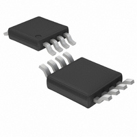
LTC1968CMS8 Linear Technology, LTC1968CMS8 Datasheet - Page 7

LTC1968CMS8
Manufacturer Part Number
LTC1968CMS8
Description
IC CONVERTER RMS-DC PREC 8MSOP
Manufacturer
Linear Technology
Datasheet
1.LTC1968CMS8PBF.pdf
(28 pages)
Specifications of LTC1968CMS8
Current - Supply
2.3mA
Voltage - Supply
5.0V
Mounting Type
Surface Mount
Package / Case
8-MSOP, Micro8™, 8-uMAX, 8-uSOP,
Lead Free Status / RoHS Status
Contains lead / RoHS non-compliant
Available stocks
Company
Part Number
Manufacturer
Quantity
Price
Company:
Part Number:
LTC1968CMS8
Manufacturer:
LT
Quantity:
10 000
Company:
Part Number:
LTC1968CMS8#TRPBF
Manufacturer:
ST
Quantity:
2 100
PI FU CTIO S
APPLICATIO S I FOR ATIO
RMS-TO-DC CONVERSION
Definition of RMS
RMS amplitude is the consistent, fair and standard way to
measure and compare dynamic signals of all shapes and
sizes. Simply stated, the RMS amplitude is the heating
potential of a dynamic waveform. A 1V
will generate the same heat in a resistive load as will 1V DC.
Mathematically, RMS is the “Root of the Mean of the
Square”:
GND (Pin 1): Ground. The power return pin.
IN1 (Pin 2): Differential Input. DC coupled (polarity is
irrelevant).
IN2 (Pin 3): Differential Input. DC coupled (polarity is
irrelevant).
V
RMS averaging is accomplished with a single shunt ca-
pacitor from Pin 5 to OUT RTN. The transfer function is
given by:
OUT
V
U
(
V
RMS
OUT
(Pin 5): Output Voltage. Pin 5 is high impedance. The
=
–
U
1V (AC + DC) RMS
OUT RTN
V
2
1V AC
1V DC
U
U
RMS
)
=
Figure 1
+
–
U
Average IN
R
R
R
1968 F01
W
⎡
⎣ ⎢
(
SAME
HEAT
RMS
2
–
AC waveform
IN
1
U
)
2
⎤
⎦ ⎥
OUT RTN (Pin 6): Output Return. The output voltage is
created relative to this pin. The V
are not balanced and this pin should be tied to a low
impedance, both AC and DC. Although Pin 6 is often tied
to GND, it can also be tied to any arbitrary voltage:
V
ENABLE (Pin 8): An Active-Low Enable Input. LTC1968 is
debiased if open circuited or driven to V
operation, pull to GND.
Alternatives to RMS
Other ways to quantify dynamic waveforms include peak
detection and average rectification. In both cases, an
average (DC) value results, but the value is only accurate
at the one chosen waveform type for which it is calibrated,
typically sine waves. The errors with average rectification
are shown in Table 1. Peak detection is worse in all cases
and is rarely used.
Table 1. Errors with Average Rectification vs True RMS
WAVEFORM
Square Wave
Sine Wave
Triangle Wave
SCR at 1/2 Power,
Θ = 90°
SCR at 1/4 Power,
Θ = 114°
The last two entries of Table 1 are chopped sine waves as
is commonly created with thyristors such as SCRs and
Triacs. Figure 2a shows a typical circuit and Figure 2b
shows the resulting load voltage, switch voltage and load
+
GND < OUT RTN < (V
(Pin 7): Positive Voltage Supply. 4.5V to 5.5V.
1.000
1.000
1.000
1.000
1.000
V
RMS
+
RECTIFIED
AVERAGE
– Max Output)
1.000
0.900
0.866
0.637
0.536
(V)
OUT
ERROR*
11%
*Calibrate for 0% Error
–3.8%
–29.3%
–40.4%
and OUT RTN pins
LTC1968
+
. For normal
7
1968f


