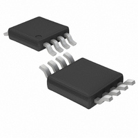
LTC1967IMS8 Linear Technology, LTC1967IMS8 Datasheet - Page 4

LTC1967IMS8
Manufacturer Part Number
LTC1967IMS8
Description
IC CONVERTER RMS-DC PREC 8MSOP
Manufacturer
Linear Technology
Datasheet
1.LTC1967CMS8.pdf
(28 pages)
Specifications of LTC1967IMS8
Current - Supply
320µA
Voltage - Supply
5.0V
Mounting Type
Surface Mount
Package / Case
8-MSOP, Micro8™, 8-uMAX, 8-uSOP,
Lead Free Status / RoHS Status
Contains lead / RoHS non-compliant
Available stocks
Company
Part Number
Manufacturer
Quantity
Price
Company:
Part Number:
LTC1967IMS8#TRPBF
Manufacturer:
LT
Quantity:
19 200
ELECTRICAL CHARACTERISTICS
LTC1967
Note 13: The common mode rejection ratios of the LTC1967 are measured
with DC inputs from 50mV to 350mV. The input CMRR is defined as the
change in V
levels of V
defined as the change in V
= V
Note 14: The LTC1967 input and output voltage swings are limited by
internal clipping. However, its
momentary internal clipping.
TYPICAL PERFOR A CE CHARACTERISTICS
4
+
– 350mV divided by V
+
IOS
– 350mV to V
measured between input levels of 0V to 350mV and input
–0.01
–0.02
–0.03
–0.04
–0.05
–0.1
–0.2
–0.3
–0.4
–0.5
–0.6
–0.7
0.05
0.04
0.03
0.02
0.01
0.3
0.2
0.1
0
0
–40
0
Gain and Offset
vs Input Common Mode Voltage
Gain and Offsets vs Temperature
50mV V
50mV V
+
OOS
+
divided by V
0.5
– 350mV.
INPUT COMMON MODE VOLTAGE (V)
measured with OUT RTN = 0V and OUT RTN
–15
1.0
IN(PEAK)
IN(PEAK)
topology is relatively tolerant of
1.5
GAIN ERROR
TEMPERATURE ( C)
W
GAIN ERROR
2.0 2.5
10
+
– 350mV. The output CMRR is
350mV
350mV
U
3.0 3.5 4.0
35
V
V
V
IOS
IOS
OOS
60
V
OOS
4.5
1967 G01
1967 G03
5.0
85
1.0
0.8
0.6
0.4
0.2
0
–0.2
–0.4
–0.6
–0.8
–1.0
0.5
0.4
0.3
0.2
0.1
0
–0.1
–0.2
–0.3
–0.4
–0.5
Note 15: The LTC1967 exploits oversampling and noise shaping to reduce
the quantization noise of internal 1-bit analog-to-digital conversions. At
higher input frequencies, increasingly large portions of this noise are
aliased down to DC. Because the noise is shifted in frequency, it becomes
a low frequency rumble and is only filtered at the expense of increasingly
long settling times. The LTC1967 is inherently wideband, but the output
accuracy is degraded by this aliased noise.
–0.1
–0.2
–0.3
–0.4
–0.5
–0.1
–0.2
–0.3
–0.4
–0.5
0.5
0.4
0.3
0.2
0.1
0.5
0.4
0.3
0.2
0.1
0
0
4.5
Gain and Offset
vs Output Common Mode Voltage
0
Gain and Offset vs Supply Voltage
GAIN ERROR
50mV V
50mV V
V
0.5
OUTPUT COMMON MODE VOLTAGE (V)
OOS
4.8
1.0
IN(PEAK)
IN(PEAK)
SUPPLY VOLTAGE (V)
1.5
2.0 2.5
5.1
V
350mV
GAIN ERROR
350mV
OOS
5.4
3.0 3.5 4.0
V
V
IOS
IOS
5.7
1967 G04
4.5
1967 G02
6.0
5.0
1.0
0.8
0.6
0.4
0.2
0
–0.2
–0.4
–0.6
–0.8
–1.0
1.0
0.8
0.6
0.4
0.2
0
–0.2
–0.4
–0.6
–0.8
–1.0
1967f


