AD637JD Analog Devices Inc, AD637JD Datasheet - Page 4
AD637JD
Manufacturer Part Number
AD637JD
Description
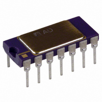
IC RMS/DC CONV PRECISION 14-CDIP
Manufacturer
Analog Devices Inc
Specifications of AD637JD
Rohs Status
RoHS non-compliant
Current - Supply
2.2mA
Voltage - Supply
±3.0V ~ 18V
Mounting Type
Through Hole
Package / Case
14-CDIP (0.300", 7.62mm)
Accuracy %
0.04%
Bandwidth
8MHz
Supply Current
2.2mA
Power Dissipation Pd
108mW
Supply Voltage Range
± 3V To ± 18V
Digital Ic Case Style
DIP
No. Of Pins
14
Operating Temperature Range
0°C
For Use With
AD637-EVALZ - BOARD EVALUATION FOR AD637
Lead Free Status / RoHS Status
Contains lead / RoHS non-compliant
Available stocks
Company
Part Number
Manufacturer
Quantity
Price

Part Number:
AD637JD
Manufacturer:
ADI/亚德诺
Quantity:
20 000


Parameter
OUTPUT CHARACTERISTICS
dB OUTPUT
BUFFER AMPLIFIER
DENOMINATOR INPUT
CHIP SELECT (CS)
POWER SUPPLY
1
2
3
4
5
6
AD637
Specifications shown in bold are tested on all production units at final electrical test. Results from those tests are used to calculate outgoing quality levels.
All minimum and maximum specifications are guaranteed, although only those shown in boldface are tested on all production units.
Accuracy specified 0 V rms to 7 V rms dc with AD637 connected, as shown in
Nonlinearity is defined as the maximum deviation from the straight line connecting the readings at 10 mV and 2 V.
Error vs. crest factor is specified as additional error for 1 V rms.
Input voltages are expressed in volts rms. Percent is in % of reading.
With external 2 kΩ pull-down resistor tied to −V
Offset Voltage
Voltage Swing,
Voltage Swing,
Output Current
Short-Circuit Current
Resistance
Resistance
Error, V
Scale Factor
Scale Factor Temperature
I
I
Input Output
Input Offset Voltage
Input Current
Input Resistance
Output Current
Short-Circuit Current
Small Signal Bandwidth
Slew Rate
Input Range
Input Resistance
Offset Voltage
RMS On Level
RMS Off Level
I
On Time Constant
Off Time Constant
Operating Voltage Range
Quiescent Current
Standby Current
REF
REF
OUT
vs. Temperature
±15 V Supply, 2 kΩ Load
±3 V Supply, 2 kΩ Load
Chip Select High
Chip Select Low
0 dB = 1 V rms
Coefficient
Voltage Range
CS Low
CS High
for 0 dB = 1 V rms
Range
of Chip Select
IN
7 mV to 7 V rms,
6
20
Min
0 to 12.0
0 to 2
6
5
1
−V
−0.13
V
±3.0
C
< 0.2 V
S
to (+V
Open or 2.4 V < V
10 + ((25 kΩ) × C
10 + ((25 kΩ) × C
AD637J/AD637A
S
− 2.5 V)
Typ
±0.05
13.5
2.2
20
0.5
100
±0.5
−3
+0.33
−0.033
20
±0.8
±2
10
20
1
5
0 to 10
25
±0.2
2.2
350
S
8
.
C
< +V
AV
AV
Max
±1
±0.089
80
100
±2
±10
+5
30
±0.5
V
10
0
±18
3
450
C
)
)
< 0.2 V
S
Rev. K | Page 4 of 20
Min
0 to 12.0
0 to 2
6
5
1
−V
−0.13
20
±3.0
S
Figure 5
to (+V
Open or 2.4 V < V
10 + ((25 kΩ) × C
10 + ((25 kΩ) × C
AD637K/AD637B
S
− 2.5 V)
.
20
20
0 to 10
25
±0.2
Typ
±0.04
13.5
2.2
0.5
100
±0.3
−3
+0.33
−0.033
20
±0.5
±2
10
1
5
V
2.2
350
C
8
< 0.2 V
C
< +V
AV
AV
Max
±0.5
±0.056
80
100
±1
±5
+5
30
±0.5
10
0
±18
3
450
)
)
S
Min
0 to 12.0
0 to 2
6
5
1
−V
−0.13
20
±3.0
S
to (+V
Open or 2.4 V < V
10 + ((25 kΩ) × C
10 + ((25 kΩ) × C
S
− 2.5 V)
Typ
±0.04
13.5
2.2
20
0.5
100
±0.5
−3
+0.33
−0.033
20
±0.8
±2
10
20
1
5
0 to 10
25
±0.2
2.2
350
AD637S
8
C
< +V
AV
AV
Max
±1
±0.07
80
100
±2
±10
+5
30
±0.5
10
0
±18
3
450
)
)
S
Unit
mV
mV/°C
V
V
mA
mA
Ω
kΩ
dB
mV/dB
% of
reading/°C
dB/°C
μA
μA
V
mV
nA
Ω
mA
mA
MHz
V/μs
V
kΩ
mV
μA
μA
μs
μs
V
mA
μA
Related parts for AD637JD
Image
Part Number
Description
Manufacturer
Datasheet
Request
R

Part Number:
Description:
BOARD EVALUATION FOR AD637
Manufacturer:
Analog Devices Inc
Datasheet:

Part Number:
Description:
±1.7g Dual-Axis IMEMS Accelerometer Evaluation Board
Manufacturer:
Analog Devices Inc
Datasheet:
Part Number:
Description:
Inertial Sensor Evaluation System
Manufacturer:
Analog Devices Inc
Datasheet:
Part Number:
Description:
Manufacturer:
Analog Devices Inc
Datasheet:
Part Number:
Description:
Manufacturer:
Analog Devices Inc
Datasheet:
Part Number:
Description:
Manufacturer:
Analog Devices Inc
Datasheet:
Part Number:
Description:
Manufacturer:
Analog Devices Inc
Datasheet:
Part Number:
Description:
Manufacturer:
Analog Devices Inc
Datasheet:
Part Number:
Description:
Manufacturer:
Analog Devices Inc
Datasheet:
Part Number:
Description:
Manufacturer:
Analog Devices Inc
Datasheet:
Part Number:
Description:
Manufacturer:
Analog Devices Inc
Datasheet:
Part Number:
Description:
Manufacturer:
Analog Devices Inc
Datasheet:
Part Number:
Description:
Manufacturer:
Analog Devices Inc
Datasheet: