AD536AJH Analog Devices Inc, AD536AJH Datasheet - Page 5
AD536AJH
Manufacturer Part Number
AD536AJH
Description
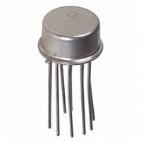
IC TRUE RMS/DC CONV TO-100-10
Manufacturer
Analog Devices Inc
Datasheet
1.AD536AJHZ.pdf
(16 pages)
Specifications of AD536AJH
Rohs Status
RoHS non-compliant
Current - Supply
1.2mA
Voltage - Supply
5.0V ~ 36V, ±3.0V ~ 18V
Mounting Type
Through Hole
Package / Case
TO-100, Metal Can (10 Leads)
Accuracy %
0.5%
Bandwidth
45kHz
Supply Current
1.2mA
Power Dissipation Pd
500mW
Supply Voltage Range
5V To 36V
Digital Ic Case Style
TO-100
No. Of Pins
10
Lead Free Status / RoHS Status
Contains lead / RoHS non-compliant
Available stocks
Company
Part Number
Manufacturer
Quantity
Price
Company:

Part Number:
AD536AJH
Manufacturer:
AD
Quantity:
5 510
Part Number:
AD536AJH
Manufacturer:
ADI/亚德诺
Quantity:
20 000
Company:
Part Number:
AD536AJHZ
Manufacturer:
AD21
Quantity:
246
Part Number:
AD536AJHZ
Manufacturer:
ADI/亚德诺
Quantity:
20 000


ABSOLUTE MAXIMUM RATINGS
Table 2.
Parameter
Supply Voltage
Internal Power Dissipation
Maximum Input Voltage
Buffer Maximum Input Voltage
Maximum Input Voltage
Storage Temperature Range
Operating Temperature Range
Lead Temperature (Soldering, 60 sec)
ESD Rating
Thermal Resistance θ
1
θ
circuit board for surface-mount packages.
JA
10-Pin Header (H-10 Package)
20-Terminal LCC (E-20 Package)
14-Lead SBDIP (D-14 Package)
14-Lead CERDIP (Q-14 Package)
Dual Supply
Single Supply
AD536AJ/AD536AK
AD536AS
is specified for the worst-case conditions, that is, a device soldered in a
JA
1
0.0807
(2.050)
1A
1B
V
V
IN
IN
1
1
PAD NUMBERS CORRESPOND TO PIN NUMBERS FOR THE
TO-100 14-LEAD CERAMIC DIP PACKAGE.
1
BOTH PADS SHOWN MUST BE CONNECTED TO V
THE AD536A IS AVAILABLE IN LASER-TRIMMED CHIP FORM.
SUBSTRATE CONNECTED TO –V
Rating
±18 V
+36 V
500 mW
±25 V peak
±V
±25 V peak
−55°C to +150°C
0°C to +70°C
−55°C to +125°C
300°C
1000 V
150°C/W
95°C/W
95°C/W
95°C/W
+V
14
S
S
Dimensions shown in inches and (millimeters)
Figure 2. Die Dimensions and Pad Layout
Rev. D | Page 5 of 16
0.1315 (3.340)
–V
3
S
S
.
Stresses above those listed under Absolute Maximum Ratings
may cause permanent damage to the device. This is a stress
rating only; functional operation of the device at these or any
other conditions above those indicated in the operational
section of this specification is not implied. Exposure to absolute
maximum rating conditions for extended periods may affect
device reliability.
ESD CAUTION
C
AV
4
COM
dB
10
5
IN
.
BUF OUT
6
R
9
L
BUF IN
I
OUT
8
7
AD536A
Related parts for AD536AJH
Image
Part Number
Description
Manufacturer
Datasheet
Request
R

Part Number:
Description:
±1.7g Dual-Axis IMEMS Accelerometer Evaluation Board
Manufacturer:
Analog Devices Inc
Datasheet:

Part Number:
Description:
Inertial Sensor Evaluation System
Manufacturer:
Analog Devices Inc
Datasheet:
Part Number:
Description:
Manufacturer:
Analog Devices Inc
Datasheet:
Part Number:
Description:
Manufacturer:
Analog Devices Inc
Datasheet:
Part Number:
Description:
Manufacturer:
Analog Devices Inc
Datasheet:
Part Number:
Description:
Manufacturer:
Analog Devices Inc
Datasheet:
Part Number:
Description:
Manufacturer:
Analog Devices Inc
Datasheet:
Part Number:
Description:
Manufacturer:
Analog Devices Inc
Datasheet:
Part Number:
Description:
Manufacturer:
Analog Devices Inc
Datasheet:
Part Number:
Description:
Manufacturer:
Analog Devices Inc
Datasheet:
Part Number:
Description:
Manufacturer:
Analog Devices Inc
Datasheet:
Part Number:
Description:
Manufacturer:
Analog Devices Inc
Datasheet:
Part Number:
Description:
Manufacturer:
Analog Devices Inc
Datasheet: