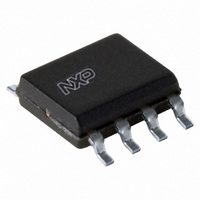
SA56004AD,112 NXP Semiconductors, SA56004AD,112 Datasheet - Page 31

SA56004AD,112
Manufacturer Part Number
SA56004AD,112
Description
IC TEMP SENSOR 8-SOIC
Manufacturer
NXP Semiconductors
Datasheet
1.SA56004BDP118.pdf
(36 pages)
Specifications of SA56004AD,112
Package / Case
8-SOIC (3.9mm Width)
Function
Temp Monitoring System (Sensor)
Topology
ADC (Sigma Delta), Multiplexer, Register Bank
Sensor Type
External & Internal
Sensing Temperature
-40°C ~ 125°C, External Sensor
Output Type
I²C™/SMBus™
Output Alarm
Yes
Output Fan
Yes
Voltage - Supply
3 V ~ 3.6 V
Operating Temperature
-40°C ~ 125°C
Mounting Type
Surface Mount
Temperature Threshold
+ 165 C
Full Temp Accuracy
1 %
Digital Output - Bus Interface
SMBus
Digital Output - Number Of Bits
11 bit
Supply Voltage (max)
3.6 V
Supply Voltage (min)
3 V
Description/function
Digital Temperature Sensor
Maximum Operating Temperature
+ 125 C
Minimum Operating Temperature
- 40 C
Supply Current
500 uA
Lead Free Status / RoHS Status
Lead free / RoHS Compliant
For Use With
568-3615 - DEMO BOARD I2C
Lead Free Status / Rohs Status
Lead free / RoHS Compliant
Other names
568-3329-5
935274525112
SA56004AD
935274525112
SA56004AD
NXP Semiconductors
SA56004X_5
Product data sheet
14.3 Wave soldering
14.4 Reflow soldering
Not all SMDs can be wave soldered. Packages with solder balls, and some leadless
packages which have solder lands underneath the body, cannot be wave soldered. Also,
leaded SMDs with leads having a pitch smaller than ~0.6 mm cannot be wave soldered,
due to an increased probability of bridging.
The reflow soldering process involves applying solder paste to a board, followed by
component placement and exposure to a temperature profile. Leaded packages,
packages with solder balls, and leadless packages are all reflow solderable.
Key characteristics in both wave and reflow soldering are:
Key characteristics in wave soldering are:
Key characteristics in reflow soldering are:
Table 20.
Package thickness (mm)
< 2.5
•
•
•
•
•
•
•
•
•
•
•
2.5
Board specifications, including the board finish, solder masks and vias
Package footprints, including solder thieves and orientation
The moisture sensitivity level of the packages
Package placement
Inspection and repair
Lead-free soldering versus SnPb soldering
Process issues, such as application of adhesive and flux, clinching of leads, board
transport, the solder wave parameters, and the time during which components are
exposed to the wave
Solder bath specifications, including temperature and impurities
Lead-free versus SnPb soldering; note that a lead-free reflow process usually leads to
higher minimum peak temperatures (see
reducing the process window
Solder paste printing issues including smearing, release, and adjusting the process
window for a mix of large and small components on one board
Reflow temperature profile; this profile includes preheat, reflow (in which the board is
heated to the peak temperature) and cooling down. It is imperative that the peak
temperature is high enough for the solder to make reliable solder joints (a solder paste
characteristic). In addition, the peak temperature must be low enough that the
packages and/or boards are not damaged. The peak temperature of the package
depends on package thickness and volume and is classified in accordance with
Table 20
SnPb eutectic process (from J-STD-020C)
and
21
Rev. 05 — 22 May 2008
Package reflow temperature ( C)
Volume (mm
< 350
235
220
Digital temperature sensor with overtemperature alarms
3
)
Figure
24) than a SnPb process, thus
220
220
350
SA56004X
© NXP B.V. 2008. All rights reserved.
31 of 36


