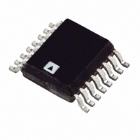
ADT7317ARQ-REEL Analog Devices Inc, ADT7317ARQ-REEL Datasheet - Page 38

ADT7317ARQ-REEL
Manufacturer Part Number
ADT7317ARQ-REEL
Description
IC SENSOR TEMP 10BIT DAC 16QSOP
Manufacturer
Analog Devices Inc
Datasheet
1.ADT7316ARQ.pdf
(44 pages)
Specifications of ADT7317ARQ-REEL
Rohs Status
RoHS non-compliant
Function
Temp Monitoring System (Sensor)
Topology
ADC, Comparator, Multiplexer, Register Bank
Sensor Type
External & Internal
Sensing Temperature
-40°C ~ 120°C, External Sensor
Output Type
I²C™, MICROWIRE™, QSPI™, SMBus™, SPI™
Output Alarm
No
Output Fan
No
Voltage - Supply
2.7 V ~ 5.5 V
Operating Temperature
-40°C ~ 120°C
Mounting Type
Surface Mount
Package / Case
16-QSOP
ADT7316/ADT7317/ADT7318
Write Operation
Figure 54 and Figure 55 show the timing diagrams for a write
operation to the ADT7316/ADT7317/ADT7318. Data is clocked
into the registers on the rising edge of SCLK. When the CS line
is high, the DIN and DOUT lines are in three-state mode. Only
when the CS goes from a high to a low does the part accept any
data on the DIN line. In SPI mode, the address pointer register
is capable of an auto-increment to the next register in the register
map without having to load the address pointer register each
SDA
SCL
SCLK
START BY
MASTER
DIN
SCLK
CS
DIN
CS
START
Figure 54. SPI—Writing to the Address Pointer Register Followed by a Single Byte of Data to the Selected Register
1
1
START
Figure 55. SPI—Writing to the Address Pointer Register to Select a Register for a Subsequent Read Operation
D7
D7
1
0
1
D6
SERIAL BUS ADDRESS BYTE
D6
0
D5
WRITE COMMAND
1
D5
Figure 53. I
WRITE COMMAND
FRAME 1
D4
A2
D4
SCLK (CONTINUED)
DIN (CONTINUED)
D3
CS (CONTINUED)
2
A1
C — Reading a Single Byte of Data From a Selected Register
D3
D2
A0
ADT7316/ADT7317/ADT7318
D2
ACKNOWLEDGE BY
R/W
D1
Rev. B | Page 38 of 44
D1
9
D0
8
D0
8
D7
1
D7
D7
SINGLE DATA BYTE FROM ADT7316/ADT7317/ADT7318
1
1
D7
time. In Figure 54, the register address section provides the first
register address that is written to. Subsequent data bytes are
written into sequential writable registers. Therefore, after each
data byte has been written into a register, the address pointer
register auto-increments its value to the next available register.
The address pointer register auto-increments from Address
0x00 to Address 0x3F and loops back to start all over again at
Address 0x00 when it reaches Address 0x3F.
1
D6
D6
D6
D6
D5
REGISTER ADDRESS
D5
D5
D5
REGISTER ADDRESS
DATA BYTE
D4
D4
D4
FRAME 2
D4
D3
D3
D3
D3
D2
NO ACKNOWLEDGE BY
D2
D2
D2
D1
D1
D1
D1
D0
D0
MASTER
D0
STOP
8
8
D0
9
8
STOP
STOP BY
MASTER


