AD580LH Analog Devices Inc, AD580LH Datasheet
AD580LH
Specifications of AD580LH
Available stocks


Related parts for AD580LH


AD580LH Summary of contents
Page 1
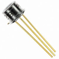
FEATURES Laser-trimmed to high accuracy: 2.500 V ±0.4% 3-terminal device: voltage in/voltage out Excellent temperature stability: 10 ppm/°C (AD580M, U) Excellent long-term stability: 250 μV (25 μV/month) Low quiescent current: 1.5 mA maximum Small, hermetic IC package: TO-52 can MIL-STD-883 ...
Page 2
AD580 TABLE OF CONTENTS Specifications..................................................................................... 3 Absolute Maximum Ratings............................................................ 4 AD580 Chip Dimensions And Pad Layout............................... 4 ESD Caution.................................................................................. 4 Theory of Operation ........................................................................ 5 Voltage Variation versus Temperature ....................................... 5 Noise Performance ....................................................................... 6 REVISION HISTORY 8/04—Changed from Rev. ...
Page 3
... Rev Page AD580L AD580M Min Typ Max Min Typ ±10 4 1.0 1.0 1 250 250 +70 0 –55 +125 –55 –65 +175 –65 AD580LH AD580MH AD580T AD580U Typ Max Min Typ Max ±10 ± 1.0 1.0 1.5 1 250 250 25 25 +125 –55 ...
Page 4
AD580 ABSOLUTE MAXIMUM RATINGS Table 3. Parameter Rating Input Voltage 40 V Power Dissipation @ 25°C Ambient Temperature 350 mW Derate above 25°C 2.8 mW/°C Lead Temperature (Soldering 300°C 10 sec) Thermal Resistance Junction-to-Case 100°C Junction-to-Ambient 360°C/W Stresses above those ...
Page 5
THEORY OF OPERATION The AD580 family (AD580, AD581, AD584, AD589) uses the bandgap concept to produce a stable, low temperature coef- ficient voltage reference suitable for high accuracy data acqui- sition components and systems. The device makes use of the ...
Page 6
AD580 The consistent voltage versus temperature performance of a typical AD580 is shown in Figure 7. Note that the characteristic is quasi-parabolic, not the possible S type characteristics of classical Zener references. This parabolic characteristic permits a maximum output deviation ...
Page 7
THE AD580 AS A LOW POWER, LOW VOLTAGE, PRECISION REFERENCE FOR DATA CONVERTERS The AD580 has a number of features that make it ideally suited for use with A/D and D/A data converters used in complex microprocessor-based systems. The calibrated ...
Page 8
... AD580 OUTLINE DIMENSIONS 0.030 (0.76) MAX ORDERING GUIDE Output Voltage Model Tolerance AD580JH ±75 mV AD580KH ±25 mV AD580LH ±10 mV AD580LMH ±10 mV AD580SH ±25 mV AD580SH/883B ±25 mV AD580TH ±10 mV AD580UH ±10 mV AD580UH/883B ±10 mV AD580TCHIPS ±10 mV © 2004 Analog Devices, Inc. All rights reserved. Trademarks and registered trademarks are the property of their respective owners ...