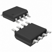
MAX6192CESA+ Maxim Integrated Products, MAX6192CESA+ Datasheet - Page 8

MAX6192CESA+
Manufacturer Part Number
MAX6192CESA+
Description
IC REF VOLT LDO 8-SOIC
Manufacturer
Maxim Integrated Products
Datasheet
1.MAX6190CESA.pdf
(14 pages)
Specifications of MAX6192CESA+
Reference Type
Series
Voltage - Output
2.5V
Tolerance
±10mV
Temperature Coefficient
25ppm/°C
Voltage - Input
2.7 ~ 12.6 V
Number Of Channels
1
Current - Quiescent
35µA
Current - Output
500µA
Operating Temperature
-40°C ~ 85°C
Mounting Type
Surface Mount
Package / Case
8-SOIC (3.9mm Width)
Product
Voltage References
Topology
Series References
Output Voltage
2.5 V
Initial Accuracy
0.4 %
Average Temperature Coefficient (typ)
25 PPM / C
Series Vref - Input Voltage (max)
12.6 V
Series Vref - Input Voltage (min)
2.69 V
Shunt Current (max)
0.5 mA
Maximum Operating Temperature
+ 85 C
Input Voltage
2.69 V to 12.6 V
Minimum Operating Temperature
- 40 C
Mounting Style
SMD/SMT
Series Vref - Supply Current (max)
35 uA
Lead Free Status / RoHS Status
Lead free / RoHS Compliant
Current - Cathode
-
Lead Free Status / Rohs Status
Lead free / RoHS Compliant
Precision, Micropower,
Low-Dropout Voltage References
ELECTRICAL CHARACTERISTICS—MAX6198
(V
8
Note 1: Temperature Coefficient is measured by the “box” method; i.e., the maximum ∆V
Note 2: Thermal Hysteresis is defined as the change in +25°C output voltage before and after cycling the device from T
Note 3: Not production tested. Guaranteed by design.
Note 4: Dropout voltage is the minimum input voltage at which V
OUTPUT
OUTPUT
DYNAMIC
DYNAMIC
INPUT
INPUT
Output Voltage
Output-Voltage Temperature
Coefficient (Note 1)
Line Regulation
Load Regulation
Dropout Voltage (Note 4)
Short-Circuit Current
Temperature Hysteresis
(Note 2)
Long-Term Stability
DYNAMIC
Noise Voltage
Ripple Rejection
Turn-On Settling Time
Capacitive-Load Stability Range
INPUT
Supply Voltage Range
Quiescent Supply Current
Change in Supply Current
IN
_______________________________________________________________________________________
= 5V, I
PARAMETER
OUT
= 0nA, T
A
= T
MIN
to T
V
SYMBOL
V
TCV
IN -
∆V
∆V
∆V
∆V
OUT
I
∆I
C
MAX
V
cycle
e
IN
∆V
time
V
I
OUT
OUT
OUT
I
OUT
OUT
OUT
SC
OUT
OUT
t
/V
IN
R
IN
V
OUT
IN
/V
OUT
, unless otherwise noted. Typical values are at T
IN
IN
/
/
/
/
MAX6198B
T
MAX6198A
MAX6198C
(V
Sourcing: 0 ≤ I
Sinking: -500µA ≤ I
∆V
Short to GND
Short to IN
1000hrs at +25°C
0.1Hz to 10Hz
10Hz to 10kHz
V
To 0.1%, C
(Note 3)
Guaranteed by line-regulation test
(V
A
IN
OUT
OUT
OUT
= +25°C
= 5V ±100mV, f = 120Hz
+ 0.2V) ≤ V
+ 0.2V) ≤ V
≤ 0.2%, I
OUT
OUT
OUT
= 50pF
CONDITIONS
OUT
IN
IN
OUT
≤ 500µA
changes ≤ 0.2% from V
≤ 12.6V
≤ 12.6V
= 500µA
≤ 0
MAX6198A
MAX6198B
MAX6198C
OUT
A
OUT
= +25°C.)
is divided by the maximum ∆t.
at V
V
4.094
4.091
4.086
OUT
MIN
IN
0
= 5.0V (V
+ 0.2
4.096
4.096
4.096
TYP
0.15
0.20
100
100
200
160
0.8
25
75
50
77
27
2
4
8
4
4
IN
= 5.5V for MAX6195).
4.098
4.101
4.106
MAX
0.70
0.90
12.6
160
200
2.2
10
25
35
5
2
MIN
to T
1000hrs
ppm/°C
UNITS
µV
µV/µA
µV
ppm/
µA/V
µV/V
ppm
mV
mA
dB
nF
µA
µs
MAX
V
RMS
V
P-P
.


