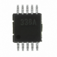
SC338AIMSTRT Semtech, SC338AIMSTRT Datasheet - Page 6

SC338AIMSTRT
Manufacturer Part Number
SC338AIMSTRT
Description
IC FET CONTROLLER DUAL 10-MSOP
Manufacturer
Semtech
Type
Positive Adjustabler
Datasheet
1.SC338AIMSTRT.pdf
(14 pages)
Specifications of SC338AIMSTRT
Number Of Outputs
2
Voltage - Output
0.5 ~ 1.8 V, 0.5 ~ 3.3 V
Current - Supply
500µA
Voltage - Input
5V, 12V
Operating Temperature
-40°C ~ 85°C
Package / Case
10-MSOP, Micro10™, 10-uMAX, 10-uSOP
Lead Free Status / RoHS Status
Lead free / RoHS Compliant
Other names
SC338AIMSTR
Theory Of Operation
The SC338(A) dual linear FET controller provides a simple
way to drive two N-channel MOSFETs to produce tightly
regulated output voltages from one or two available,
higher, supply voltages. It takes its power from either a
5V or 12V supply, drawing typically 500µA while
operating.
It contains an internal bandgap reference which is
compared to the output voltages via resistor dividers.
These resistor dividers are external and user selectable .
Depending upon the input voltage used for the device,
the drive pin (DRV1, DRV2) can pull up to a guaranteed
minimum of 6.6V (from 12V supply) or 4.7V (from 5V
supply). Thus the device can be used to regulate a large
range of output voltages by careful selection of the
external MOSFETs (see component selection, below).
The SC338(A) includes an active high enable control (EN1,
EN2) for each output. If this pin is pulled low, the related
drive pin is pulled low, turning off the N-channel MOSFET.
If the pin is pulled up to 1.8V
be enabled. This pin should not be allowed to float.
Each output has a power good output (PGD1, PGD2)
which are open drain outputs that pull low if the related
output is below the power good threshold (-12% of the
programmed output voltage typical, -6% typical at start-
up). The power good circuitry is active if the device is
enabled, regardless of the state of the over current latch.
The power good circuitry is not active if that
particular output is disabled.
Also included for each output is an overcurrent
protection circuit that monitors the output voltage. If the
output voltage drops below 50% (typ.) of nominal, as
would occur during an overcurrent or short condition, the
device will pull the drive pin low and latch off. The device
will need to have the power supply or enable pin toggled
to reset the latch condition. Each output latches
independently (i.e. if one output latches off, the other
output will function normally).
Drive Outputs and Soft Start
The drive outputs for each output are source and sink
capable. The sink current is typically 0.8mA at 5V in (1mA
at 12V in). The source current is typically 2mA at 5V in
POWER MANAGEMENT
Applications Infomation
2004 Semtech Corp.
V
EN
V
IN
, the drive pin will
6
and 3.75mA at 12V in during normal operation. The high
side drive voltage is generated from V
low dropout regulator, thus at 12V in, 6.9V is available
and at 5V in, 4.85V is available (since the LDO will be in
dropout).
At start-up, the source current available from the drive
pins is limited to 10µA (typical) until the power good
threshold is reached, at approximately 6% below
nominal output voltage. At this point the full drive
capability is enabled. With this constant current source
at start-up, it is a simple matter to use a small capacitor
on the drive pin to slow this rate of rise. The rate of rise
of the drive pin voltage will be:
A 10nF soft start capacitor will give a 1ms output rise
time for V
output rise time will of course depend upon the gate
threshold of the MOSFET being used. Please refer to
the Output Rise Time chart on Page 13 showing typical
output rise times. For very low ESR output capacitors
(<5m ) and very high soft start capacitance (>100nF),
it may be necessary to add a resistor in series with the
soft start capacitor to ensure stability. Generally,
however, this resistor is not required, as this is a very
unlikely situation.
The soft start capacitance does not adversely affect
transient response since the drive current capability is
200 times higher once the device has started.
OCP and Power Supply Sequencing
The SC338(A) has output undervoltage protection that
looks at a particular output to see if it is a) less than
50% (typical) of it’s nominal value and b) V
output is within 350mV (typical) of maximum. If both of
these criteria are met, there is a 50µs (typical) delay and
then the output is shut down. This provides inherent
immunity to UV shutdown at start-up (which may occur
while the output capacitors are being charged) since V
has a very slow rate of rise with I
At start-up, it is necessary to ensure that the power
supplies and enables are sequenced correctly to avoid
erroneous latch-off. For UV latch-off not to occur at start-
up due to sequencing issues, the key is that the voltage
dV
dt
DRV
I
C
DRV
IN
SS
= 12V and V
V
s /
OUT
= 1.05V, for example. The
DRV
limited to 10µA.
IN
PRELIMINARY
SC338(A)
by a 7V (nominal)
www.semtech.com
DRV
for that
DRV


