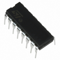
SG3524N STMicroelectronics, SG3524N Datasheet - Page 5

SG3524N
Manufacturer Part Number
SG3524N
Description
IC PWM REGULATING 16-DIP
Manufacturer
STMicroelectronics
Type
Pulse Width Modulator Controllerr
Specifications of SG3524N
Pwm Type
Voltage Mode
Number Of Outputs
1
Frequency - Max
300kHz
Duty Cycle
45%
Voltage - Supply
8 V ~ 40 V
Buck
No
Boost
No
Flyback
Yes
Inverting
No
Doubler
Yes
Divider
No
Cuk
No
Isolated
No
Operating Temperature
0°C ~ 70°C
Package / Case
16-DIP (0.300", 7.62mm)
Frequency-max
300kHz
Topology
Push-Pull
Output Voltage
18 V
Output Current
100 mA
Switching Frequency
300 KHz
Duty Cycle (max)
45 %
Maximum Operating Temperature
+ 70 C
Minimum Operating Temperature
0 C
Fall Time
100 ns
Mounting Style
Through Hole
Rise Time
200 ns
Synchronous Pin
No
Common Mode Rejection Ratio
70
Current, Input Bias
2 μA
Current, Output
100 mA
Current, Supply
8 mA
Frequency, Oscillator
300 kHz
Package Type
DIP-16
Power Dissipation
1000 mW
Regulation, Line
10 mV
Regulation, Load
20 mV
Temperature, Operating, Range
0 to +70 °C
Time, Fall
0.1 μs
Time, Rise
0.2 μs
Voltage, Gain
80 dB
Voltage, Input
20 V
Voltage, Offset
2 mV
Voltage, Output
5 V
Voltage, Supply
8 to 40 V
Lead Free Status / RoHS Status
Contains lead / RoHS non-compliant
Other names
497-2992-5
Available stocks
Company
Part Number
Manufacturer
Quantity
Price
Part Number:
SG3524N
Manufacturer:
TI/德州仪器
Quantity:
20 000
Part Number:
SG3524NSR
Manufacturer:
TI/德州仪器
Quantity:
20 000
PRINCIPLES OF OPERATION
The SG3524 is a fixed frequency pulse-with-
modulation voltage regulator control circuit. The
regulator operates at a frequency that is pro-
grammed by one timing resistor (R
ing capacitor (C
charging current for C
voltage ramp at C
tor providing linear control of the output pulse
width by the error amplifier. the SG3524 contains,
an on-board 5V regulator that serves as a refer-
ence as well as powering the SG3524’s internal
control circuitry and is also useful in supplying ex-
ternal support functions. This reference voltage is
lowered externally by a resistor divider to provide
a reference within the common mode range the
error amplifier or an external reference may be
used. The power supply output is sensed by a
second resistor divider network to generale a
feedback signal to error amplifier. The amplifier
output voltage is then compared to the linear volt-
age ramp at C
out of the high-gain comparator is then steered to
the appropriate output pass transistors (Q
by the pulse-steering flip-flop, which is synchro-
nously toggled by the oscillator output. The oscil-
lator output pulse also serves as a blanking pulse
to assure both output are never on simultane-
ously during the transition times. The width of the
blanking pulse is controlled by the value of C
The outputs may be applied in a push-pull con-
figuration in which their frequency is half that of
the base oscillator, or paralleled for single-ended
applications in which the frequency is equal to
that of the oscillator. The output of the error am-
plifier shares a common input to the comparator
with the current limiting at shutdown circuitry and
can be overridden by signals from either of these
inputs. This common point is also available exter-
nally and may be employed to control the gain of,
or to compensate, the error amplifier, or to pro-
vide additional control to the regulator.
RECOMMENDED OPERATING CONDITIONS
TYPICAL APPLICATIONS DATA
OSCILLATOR
The oscillator controls the frequency of the
SG3524 and is programmed by R
Supply voltage V
Reference Output Current
Current trough C
Timing Resistor, R
Timing Capacitor, C
T
T
IN
. The resulting modulated pulse
Terminal
T
T
T
). R
T
, which is fed to the compara-
T
T
. This results in a linear
established a constant
0.001 to 0.1 F
- 0.03 to -2mA
1.8 to 100K
0 to 20mA
T
8 to 40V
) and one tim-
T
and C
A
or Q
T
ac-
B
T
)
.
cording to the approximate formula:
where:
R
C
f is in KHz
Pratical values of C
0.1 F. Pratical values of R
100K . This results in a frequency range typically
from 120Hz to to 500KHz.
BLANKING
The output pulse of oscillator is used as a blank-
ing pulse at the output. This pulse width is con-
trolled by the value of C
required for frequency control, the oscillator out-
put pulse width may still be increased by applying
a shunt capacitance of up to 100pF from pin 3 to
ground. If still greater dead-time is required, it
should be accomplished by limiting the maximum
duty cycle by clamping the output of the error am-
plifier. This can easily be done with the circuit be-
low:
Figure 6.
SYNCRONOUS OPERATION
When an external clock is desired, a clock pulse
of approximately 3V can be applied directly to the
oscillator output terminal. The impedance to
ground at this point is approximately 2K . In this
configuration R
period slightly greater than that the external clock.
If two more SG2524 regulators are to be operated
synchronously, all oscillator output terminals
should be tied together, all C
nected to a single timing capacitor, and timing re-
sistor connected to a single R
other R
V
tween the C
REF
T
T
is in K
is in F
. Minimum lead lengths should be used be-
T
terminals can be left open or shorted to
T
terminals.
T
C
T
f
must be selected for a clock
T
R
T
1.18
fall between 0.001 and
.If small values of C
T
C
T
T
fall between 1.8 and
T
T
terminals con-
terminal. The
SG3524
T
are
5/9


