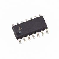
HIP6012CBZ Intersil, HIP6012CBZ Datasheet - Page 6

HIP6012CBZ
Manufacturer Part Number
HIP6012CBZ
Description
IC CTRLR PWM BUCK SYNC 14-SOIC
Manufacturer
Intersil
Datasheet
1.HIP6012CBZ-T.pdf
(12 pages)
Specifications of HIP6012CBZ
Pwm Type
Voltage Mode
Number Of Outputs
1
Frequency - Max
1MHz
Duty Cycle
100%
Voltage - Supply
2.5 V ~ 12 V
Buck
Yes
Boost
No
Flyback
No
Inverting
No
Doubler
No
Divider
No
Cuk
No
Isolated
No
Operating Temperature
0°C ~ 70°C
Package / Case
14-SOIC (3.9mm Width), 14-SOL
Frequency-max
1MHz
Lead Free Status / RoHS Status
Lead free / RoHS Compliant
Available stocks
Company
Part Number
Manufacturer
Quantity
Price
Part Number:
HIP6012CBZ
Manufacturer:
HARRIS
Quantity:
20 000
Part Number:
HIP6012CBZ-TR5226
Manufacturer:
INTERSIL
Quantity:
20 000
complete its cycle. Figure 4 shows this operation with an
overload condition. Note that the inductor current increases
to over 15A during the C
overcurrent trip. The converter dissipates very little power
with this method. The measured input power for the
conditions of Figure 4 is 2.5W.
The overcurrent function will trip at a peak inductor current
(I
where I
- typical). The OC trip point varies mainly due to the
MOSFETs r
in the normal operating load range, find the R
from the equation above with:
For an equation for the ripple current see the section under
component guidelines titled ‘Output Inductor Selection’.
A small ceramic capacitor should be placed in parallel with
R
presence of switching noise on the input voltage.
Application Guidelines
Layout Considerations
As in any high frequency switching converter, layout is very
important. Switching current from one power device to
another can generate voltage transients across the
impedances of the interconnecting bond wires and circuit
traces. These interconnecting impedances should be
minimized by using wide, short printed circuit traces. The
critical components should be located as close together as
possible using ground plane construction or single point
grounding.
Figure 5 shows the critical power components of the
converter. To minimize the voltage overshoot the
interconnecting wires indicated by heavy lines should be part
of ground or power plane in a printed circuit board. The
components shown in Figure 6 should be located as close
together as possible. Please note that the capacitors C
and C
Locate the HIP6012 within 3 inches of the MOSFETs, Q1
and Q2. The circuit traces for the MOSFETs’ gate and
source connections from the HIP6012 must be sized to
handle up to 1A peak current.
Figure 6 shows the circuit traces that require additional
layout consideration. Use single point and ground plane
construction for the circuits shown. Minimize any leakage
current paths on the SS PIN and locate the capacitor, C
I
1. The maximum r
2. The minimum I
3. Determine
PEAK
PEAK)
OCSET
where ∆I is the output inductor ripple current.
O
=
OCSET
determined by:
each represent numerous physical capacitors.
to smooth the voltage across R
I
-------------------------------------------------- -
OCSET
DS(ON)
r
DS ON
is the internal OCSET current source (200µA
I
PEAK
•
(
R
OCSET
DS(ON)
variations. To avoid overcurrent tripping
OCSET
)
for I
SS
PEAK
from the specification table.
at the highest junction temperature.
charging interval and causes an
6
>
I
OUT MAX
(
OCSET
)
+
OCSET
(
∆I
in the
) 2 ⁄
,
resistor
IN
SS
HIP6012
close to the SS pin because the internal current source is
only 10µA. Provide local V
GND pins. Locate the capacitor, C
to the BOOT and PHASE pins.
Feedback Compensation
Figure 7 highlights the voltage-mode control loop for a
synchronous-rectified buck converter. The output voltage
(V
amplifier (Error Amp) output (V
oscillator (OSC) triangular wave to provide a pulse-width
modulated (PWM) wave with an amplitude of V
PHASE node. The PWM wave is smoothed by the output filter
(L
The modulator transfer function is the small-signal transfer
function of V
Gain and the output filter (L
break frequency at F
the modulator is simply the input voltage (V
peak-to-peak oscillator voltage ∆V
O
OUT
FIGURE 5. PRINTED CIRCUIT BOARD POWER AND
C
FIGURE 6. PRINTED CIRCUIT BOARD SMALL SIGNAL
SS
HIP6012
SS
and C
) is regulated to the Reference voltage level. The error
HIP6012
O
UGATE
PHASE
GND
LGATE
).
PGND
OUT
GROUND PLANES OR ISLANDS
LAYOUT GUIDELINES
/V
E/A
LC
PHASE
C
VCC
BOOT
. This function is dominated by a DC
BOOT
and a zero at F
+12V
CC
V
Q2
Q1
O
RETURN
IN
C
and C
decoupling between VCC and
VCC
E/A
D1
D2
BOOT
OSC
) is compared with the
O
), with a double pole
.
ESR
C
as close as practical
Q1
+V
IN
Q2
IN
IN
L
. The DC Gain of
O
L
) Divided by the
C
O
IN
December 27, 2004
C
O
O
at the
V
OUT
FN4324.2
V
OUT


