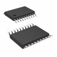
LM5034MTC/NOPB National Semiconductor, LM5034MTC/NOPB Datasheet - Page 5

LM5034MTC/NOPB
Manufacturer Part Number
LM5034MTC/NOPB
Description
IC CTRLR PWM DUAL CMODE 20TSSOP
Manufacturer
National Semiconductor
Series
PowerWise®r
Datasheet
1.LM5034MTCNOPB.pdf
(29 pages)
Specifications of LM5034MTC/NOPB
Pwm Type
Current Mode
Number Of Outputs
2
Frequency - Max
1MHz
Duty Cycle
94%
Voltage - Supply
13 V ~ 100 V
Buck
Yes
Boost
Yes
Flyback
No
Inverting
Yes
Doubler
No
Divider
No
Cuk
No
Isolated
Yes
Operating Temperature
-40°C ~ 125°C
Package / Case
20-TSSOP
Frequency-max
2MHz
For Use With
LM5034EVAL - BOARD EVALUATION LM5034
Lead Free Status / RoHS Status
Lead free / RoHS Compliant
Other names
*LM5034MTC
LM5034MTC
LM5034MTC
Absolute Maximum Ratings
If Military/Aerospace specified devices are required,
please contact the National Semiconductor Sales Office/
Distributors for availability and specifications.
Electrical Characteristics
VIN to GND
VCC to GND
RT/SYNC, RES and DCL to GND
CS Pins to GND
All other inputs to GND
ESD Rating (Note 5)
Specifications with standard typeface are for T
Temperature range. VIN = 48V, VCC1 = VCC2 = 10V externally applied, R
1.5V, unless otherwise stated (Note 3) and (Note 4).
Startup Regulator (VIN, VCC1, VCC2 Pins)
V
I
V
I
I
UVLO
UVLO
I
Current Sense Input (CS1, CS2 Pins)
CS
R
Current Limit Restart (RES Pin)
ResTh
Soft-start (SS1, SS2 Pins)
I
V
CC(Lim)
IN
CC
HYST
SS
CC
CC
SS
CS
Human Body Model
Symbol
In
Reg
UVT
V
V
V
(V
V
Startup regulator current
Supply current into VCC
from external source
Under-voltage threshold
Hysteresis current
Current Limit Threshold
CS delay to output
Leading edge blanking time
at CS1 (CS2)
CS1 (CS2) sink impedance
(clocked)
Equivalent input resistance
at CS
Threshold
Charge source current
Discharge sink current
Current source (normal
operation)
Current source during a
current limit restart
Open circuit voltage
CC
CC
CC
CC
CC
voltage
current limit
Under-voltage threshold
decreasing
increasing)
Parameter
-0.3V to 105V
-0.3V to 16V
-0.3V to 5.5V
-0.3V to 1.25V
-0.3V to 7V
2kV
VCC1 connected to VCC2, ext. supply
disconnected.
Sum of currents out of VCC1 and VCC2
with VCC1 = VCC2 = 0V.
VCC1 connected to VCC2, ext. supply
disconnected, VIN =11V.
VIN = 90V, UVLO = 0V
Output loads = open, V
CS1 (CS2) taken from zero to 1.0V.
Time for OUT1 (OUT2) to fall to 90% of
VCC1 (VCC2). Output load = 0 pF.
Internal pull-down FET on.
CS taken from 0.2V to 0.5V, internal
FET off.
(Note 1)
J
= 25˚C, and those with boldface type apply over full Operating Junction
Conditions
5
Operating Ratings
Storage Temperature Range
Junction Temperature
Lead Temperature (Soldering 4 sec),
(Note 2)
VIN Voltage
External Voltage Applied to VCC1,
VCC2
Operating Junction Temperature
CC
= 10V
T
= R
DCL
= 42.2kΩ, R
300 mV
VCC -
1.22
0.45
Min
7.4
5.5
2.4
7.5
0.7
19
16
15
35
(Note 1)
OVLP
100 mV
VCC -
1.25
2.55
Typ
500
7.7
6.2
4.3
0.5
22
20
40
50
30
42
20
10
50
1
5
=70kΩ, UVLO =
-55˚C to 150˚C
150˚C
260˚C
-40˚C to +125˚C
Max
1.28
0.55
12.5
600
6.9
2.7
1.3
24
55
25
65
8
7
13.0V to 100V
www.national.com
8V to 15V
Units
mA
mA
µA
µA
kΩ
µA
µA
µA
µA
ns
ns
Ω
V
V
V
V
V
V
V


