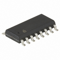
ISL6721ABZ Intersil, ISL6721ABZ Datasheet - Page 9

ISL6721ABZ
Manufacturer Part Number
ISL6721ABZ
Description
IC CTRLR PWM SGL ENDED 16-SOIC
Manufacturer
Intersil
Datasheet
1.ISL6721ABZ.pdf
(22 pages)
Specifications of ISL6721ABZ
Pwm Type
Current Mode
Number Of Outputs
1
Frequency - Max
1MHz
Duty Cycle
100%
Voltage - Supply
9 V ~ 18 V
Buck
Yes
Boost
Yes
Flyback
Yes
Inverting
No
Doubler
No
Divider
No
Cuk
No
Isolated
Yes
Operating Temperature
-40°C ~ 105°C
Package / Case
16-SOIC (3.9mm Width)
Frequency-max
1MHz
Peak Reflow Compatible (260 C)
Yes
Rohs Compliant
Yes
Lead Free Status / RoHS Status
Lead free / RoHS Compliant
Available stocks
Company
Part Number
Manufacturer
Quantity
Price
Company:
Part Number:
ISL6721ABZ
Manufacturer:
Intersil
Quantity:
135
Company:
Part Number:
ISL6721ABZ
Manufacturer:
Intersil
Quantity:
500
Part Number:
ISL6721ABZ
Manufacturer:
INTERSIL
Quantity:
20 000
Part Number:
ISL6721ABZ-T
Manufacturer:
INTERSIL
Quantity:
20 000
Pin Descriptions
SLOPE - Means by which the ISENSE ramp slope may be
increased for improved noise immunity or improved control
loop stability for duty cycles greater than 50%. An internal
current source charges an external capacitor to GND during
each switching cycle. The resulting ramp is scaled and
added to the ISENSE signal.
SYNC - A bidirectional synchronization signal used to
coordinate the switching frequency of multiple units.
Synchronization may be achieved by connecting the SYNC
signal of each unit together or by using an external master
clock signal. The oscillator timing capacitor, C
required, even if an external clock is used. The first unit to
assert this signal assumes control.
RTCT - This is the oscillator timing control pin. The
operational frequency and maximum duty cycle are set by
connecting a resistor, R
timing capacitor, C
produces a sawtooth waveform with a programmable
frequency range of 100kHz to 1.0MHz. The charge time, t
the discharge time, t
maximum duty cycle, Dmax, can be calculated from
Equations 1, 2, 3 and 4:
Dmax
Figure 4 may be used as a guideline in selecting the
capacitor and resistor values required for a given frequency.
COMP - COMP is the output of the error amplifier and the
input of the PWM comparator. The control loop frequency
compensation network is connected between the COMP and
FB pins.
The ISL6721 features a built-in full cycle soft-start. Soft-start
is implemented as a clamp on the maximum COMP voltage.
FB - Feedback voltage input connected to the inverting input
of the error amplifier. The non-inverting input of the error
amplifier is internally tied to a reference voltage. Current
sense leading edge blanking is disabled when the FB input
is less than 2.0V.
OV - Overvoltage monitor input pin. This signal is compared
to an internal 2.5V reference to detect an overvoltage
condition.
t
t
f
D
sw
C
≈
≈
=
0.655 R T C T
–
R
---------------- -
t
=
T
D
•
1
+
t
C
•
C
t
C
•
T
f
sw
•
•
LN
Hz
⎛
⎝
T
0.001 R T 3.6
------------------------------------------ -
0.001 R T 1.9
, from this pin to LGND. The oscillator
D
, the switching frequency, f sw , and the
T
S
•
•
, between V
–
–
9
⎞
⎠
REF
S
and this pin and a
T
, is still
(EQ. 1)
(EQ. 2)
(EQ. 3)
(EQ. 4)
C
,
ISL6721
UV - Undervoltage monitor input pin. This signal is
compared to an internal 1.45V reference to detect an
undervoltage condition.
ISENSE - This is the input to the current sense comparators.
The IC has two current sensing comparators, a PWM
comparator for peak current mode control, and an
overcurrent protection comparator. The overcurrent
comparator threshold is adjustable through the ISET pin.
Exceeding the overcurrent threshold will start a delayed
shutdown sequence. Once an overcurrent condition is
detected, the soft-start charge current source is disabled and
a discharge current source is enabled. The soft-start capacitor
begins discharging, and if it discharges to less than 4.375V
(sustained overcurrent threshold), a shutdown condition
occurs and the GATE output is forced low. At this point a
reduced discharge current takes over until the soft-start
voltage reaches 0.27V (reset threshold). The GATE output
remains low until the reset threshold is attained. At this point,
a soft-start cycle begins.
If the overcurrent condition ceases, and then an additional
50µs period elapses before the shutdown threshold is
reached, no shutdown occurs and the soft-start voltage is
allowed to recharge.
LGND - LGND is a small signal reference ground for all
analog functions on this device.
PGND - This pin provides a dedicated ground for the output
gate driver. The LGND and PGND pins should be connected
externally using a short printed circuit board trace close to
the IC. This is imperative to prevent large, high frequency
switching currents flowing through the ground metallization
inside the IC. (Decouple V
or larger capacitor.)
GATE - This is the device output. It is a high current power
driver capable of driving the gate of a power MOSFET with
peak currents of 1.0A. This GATE output is actively held low
when V
The output high voltage is clamped to ~13.5V. Voltages
exceeding this clamp value should not be applied to the
GATE pin. The output stage provides very low impedance to
overshoot and undershoot.
VC - This pin is for separate collector supply to the output
gate drive. Separate V
analog circuitry from the high power gate drive noise.
(Decouple V
capacitor.)
VCC - V
quiescent current, I
frequency of operation. To optimize noise immunity, bypass
V
and LGND pins as possible.
CC
to LGND with a ceramic capacitor as close to the V
CC
CC
is below the UVLO threshold.
is the power connection for the device. Although
C
to PGND with a low ESR 0.1µF or larger
CC
, is low, it is dependent on the
C
and PGND helps decouple the IC’s
C
to PGND with a low ESR 0.1µF
March 5, 2008
FN9110.6
CC


