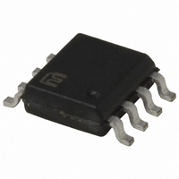
MIC2196YM TR Micrel Inc, MIC2196YM TR Datasheet - Page 10

MIC2196YM TR
Manufacturer Part Number
MIC2196YM TR
Description
IC PWM BST FLYBCK CM 8SOIC
Manufacturer
Micrel Inc
Datasheet
1.MIC2196YM.pdf
(12 pages)
Specifications of MIC2196YM TR
Pwm Type
Current Mode
Number Of Outputs
1
Frequency - Max
440kHz
Duty Cycle
85%
Voltage - Supply
2.9 V ~ 14 V
Buck
No
Boost
Yes
Flyback
Yes
Inverting
No
Doubler
No
Divider
No
Cuk
No
Isolated
No
Operating Temperature
-40°C ~ 125°C
Package / Case
8-SOIC (3.9mm Width)
Frequency-max
440kHz
Lead Free Status / RoHS Status
Lead free / RoHS Compliant
Other names
MIC2196YMTR
MIC2196YMTR
MIC2196YMTR
The enable pin (pin 3) has two threshold levels, allowing
the MIC2196 to shut down in a micro-current mode, or
turn-off output switching in standby mode. Below 0.9V,
the device is forced into a micro power shutdown. If the
enable pin is between 0.9V and 1.5V the output gate
drive is disabled but the internal circuitry is powered on
and the soft start pin voltage is forced low. There is
typically 135mV of hysteresis below the 1.5V threshold
to insure the part does not oscillate on and off due to
ripple voltage on the input. Raising the enable voltage
above the UVLO threshold of 1.5V enables the output
drivers and allows the soft start capacitor to charge. The
enable pin may be pulled up to VINA.
Oscillator and Sync
The internal oscillator is self-contained and requires no
external components. The maximum duty cycle of the
MIC2196 is 85%.
Minimum duty cycle becomes important in a boost
converter as the input voltage approaches the output
voltage. At lower duty cycles, the input voltage can be
closer to the output voltage without the output rising out
of regulation. Minimum duty cycle is typically 7%.
A frequency foldback mode is enabled if the voltage on
the feedback pin (pin 2) is less than 0.3V. In frequency
foldback
approximately a factor of 4.
Voltage Setting Components
The MIC2196 requires two resistors to set the output
voltage as shown in Figure 5.
The output voltage is determined by the equation below:
Where: V
Lower values of resistance are preferred to prevent
noise from appearing on the V
recommended value for R1 is 10K.
Micrel, Inc.
September 2008
V
REF
Figure 5. Voltage Setting Components
O
the
=
for the MIC2196 is nominally 1.245V.
V
REF
oscillator
×
1.245V
1
Amplifier
Voltage
MIC2196
V
+
REF
R2
R1
frequency
Pin
6
FB
R1
R2
is
pin. A typically
reduced
by
10
Decoupling Capacitor Selection
A 1μF decoupling capacitor is used to stabilize the
internal regulator and minimize noise on the V
Placement of this capacitor is critical to the proper
operation of the MIC2196. It must be next to the V
signal ground pins and routed with wide etch. The
capacitor should be a good quality ceramic. Incorrect
placement of the V
jitter and/or oscillations in the switching waveform as
well as variations in the overcurrent limit.
A minimum 1μF ceramic capacitor is required to
decouple the V
the IC and connected directly between pins 8 (V
6 (GND). For V
ceramic capacitor to decouple the V
Efficiency Calculation and Considerations
Efficiency is the ratio of output power to input power. The
difference is dissipated as heat in the boost converter.
The significant contributors at light output loads are:
To maximize efficiency at light loads:
The significant contributors to power loss at higher
output loads are (in approximate order of magnitude):
To minimize power loss under heavy loads:
•
•
•
•
•
•
•
•
•
•
•
The VIN pin supply current which includes the
current
MOSFETs.
Core losses in the inductor.
Use a low gate charge MOSFET or use the
smallest MOSFET, which is still adequate for the
maximum output current.
Use a ferrite material for the inductor core, which
has less core loss than an MPP or iron power
core.
Resistive on-time losses in the MOSFET
Switching transition losses in the MOSFET
Inductor resistive losses
Current sense resistor losses
Output capacitor resistive losses (due to the
capacitor’s ESR)
Use logic level, low on resistance MOSFETs.
Multiplying the gate charge by the on-resistance
gives a figure of merit, providing a good balance
between
dissipation.
Slow transition times and oscillations on the
voltage and current waveforms dissipate more
power during the turn-on and turn-off of the low
side MOSFET. A clean layout will minimize
parasitic inductance and capacitance in the gate
drive and high current paths. This will allow the
IN
IN
. The capacitor should be placed near
greater than 8V, use a 4.7μF or a 10μF
required
switching
DD
decoupling capacitor will cause
to
and
switch
DD
pin.
resistive
M9999-092908
the
MIC2196
external
CC
DD
DD
power
) and
and
pin.


