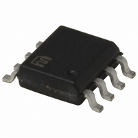
MIC2193YM Micrel Inc, MIC2193YM Datasheet - Page 7

MIC2193YM
Manufacturer Part Number
MIC2193YM
Description
IC PWM BUCK CM 8SOIC
Manufacturer
Micrel Inc
Datasheet
1.MIC2193YM_TR.pdf
(10 pages)
Specifications of MIC2193YM
Pwm Type
Current Mode
Number Of Outputs
1
Frequency - Max
440kHz
Duty Cycle
100%
Voltage - Supply
2.9 V ~ 14 V
Buck
Yes
Boost
No
Flyback
No
Inverting
No
Doubler
No
Divider
No
Cuk
No
Isolated
No
Operating Temperature
-40°C ~ 125°C
Package / Case
8-SOIC (3.9mm Width)
Frequency-max
440kHz
Lead Free Status / RoHS Status
Lead free / RoHS Compliant
Available stocks
Company
Part Number
Manufacturer
Quantity
Price
Part Number:
MIC2193YM
Manufacturer:
MICREL/麦瑞
Quantity:
20 000
Company:
Part Number:
MIC2193YM-TR
Manufacturer:
YD
Quantity:
6 224
The MIC2193 controller is broken down into five functions.
• Control loop
• Current limit
• Reference and V
• MOSFET gate drive
• Oscillator
Control Loop
PWM Control Loop
The MIC2193 uses current mode control to regulate the
output voltage. This dual control loop method (illustrated in
Figure 2) senses the output voltage (outer loop) and the
inductor current (inner loop). It uses inductor current and
output voltage to determine the duty cycle of the buck
converter. Sampling the inductor current effectively removes
the inductor from the control loop, which simplifies compen-
sation.
As shown in Figure 1, the inductor current is sensed by
measuring the voltage across the resistor, R
added to the amplified current sense signal to provide slope
compensation, which is required to prevent unstable opera-
tion at duty cycles greater than 50%.
A transconductance amplifier is used for the error amplifier,
which compares an attenuated sample of the output voltage
with a reference voltage. The output of the error amplifier is
the compensation pin (COMP), which is compared to the
current sense waveform in the PWM block. When the current
signal becomes greater than the error signal, the comparator
turns off the high-side drive. The COMP pin provides access
to the output of the error amplifier and allows the use of
external components to stabilize the voltage loop.
April 2004
MIC2193
- PWM operation
- Current mode control
Figure 2. Current Mode Control Example
V
IN
V
Converter
ERROR
Switching
Switch
Driver
t
PER
t
ON
I
INDUCTOR
DD
D = t
V
ON
ERROR
/t
PER
I
INDUCTOR
V
SENSE
REF
Voltage
Divider
V
OUT
. A ramp is
7
Current Limit
The output current is detected by the voltage drop across the
external current sense resistor (R
current sense resistor must be sized using the minimum
current limit threshold. The external components must be
designed to withstand the maximum current limit. The current
sense resistor value is calculated by the equation below:
The maximum output current is:
The current sense pins VIN (pin 1) and CSL (pin 4) are noise
sensitive due to the low signal level and high input impedance
and switching noise on the VIN pin. The PCB traces should
be short and routed close to each other. A 10nF capacitor
across the pins will attenuate high frequency switching noise.
When the peak inductor current exceeds the current limit
threshold, the overcurrent comparator turns off the high side
MOSFET for the remainder of the switching cycle, effectively
decreasing the duty cycle. The output voltage drops as
additional load current is pulled from the converter. When the
voltage at the feedback pin (FB) reaches approximately 0.3V,
the circuit enters frequency foldback mode and the oscillator
frequency will drop to approximately 1/4 of the switching
frequency. This limits the maximum output power delivered to
the load under a short circuit condition.
Reference and V
The output drivers are enabled when the V
is greater than its undervoltage threshold.
The internal bias circuit generates an internal 1.245V band-
gap reference voltage for the voltage error amplifier and a 3V
V
must be decoupled with a 1 F ceramic capacitor. The capaci-
tor must be placed close to the VDD pin. The other end of the
capacitor must be connected directly to the ground plane.
MOSFET Gate Drive
The MIC2193 is designed to drive a high-side, P-Channel
MOSFET and a low side, N-Channel MOSFET. The source
pin of the P-channel MOSFET is connected to the input of the
power supply. It is turned on when OUTP pulls the gate of the
MOSFET low. The advantage of using a P-channel MOSFET
is that it does not required a bootstrap circuit to boost the gate
voltage higher than the input, as would be required for an N-
channel MOSFET.
The VIN pin (pin 1) supplies the drive voltage to both gate
drive pins, OUTN and OUTP. The VIN pin must be well
decoupled to prevent noise from affecting the current sense
circuit, which uses VIN as one of the sense pins.
A non-overlap time is built into the MOSFET driver circuitry.
This dead time prevents the high-side and low-side MOSFET
drivers from being on at the same time. Either an external
diode or the low-side MOSFET internal parasitic diode con-
ducts the inductor current during the dead time.
DD
voltage for the internal control circuitry. The VDD pin
R
I
OUT MAX
SENSE
_
MIN CURRENT SENSE THRESHOLD
MAX CURRENT SENSE THRESHOLD
_
DD
_
Circuits
I
OUT MAX
_
R
_
_
SENSE
SENSE
_
_
in Figure 1.). The
DD
voltage (pin 5)
M9999-042704
Micrel


