LM5034MTCX/NOPB National Semiconductor, LM5034MTCX/NOPB Datasheet - Page 6
LM5034MTCX/NOPB
Manufacturer Part Number
LM5034MTCX/NOPB
Description
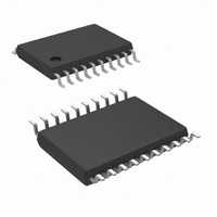
IC CTLR PWM DUAL CMODE 20TSSOP
Manufacturer
National Semiconductor
Series
PowerWise®r
Datasheet
1.LM5034MTCNOPB.pdf
(29 pages)
Specifications of LM5034MTCX/NOPB
Pwm Type
Current Mode
Number Of Outputs
2
Frequency - Max
1MHz
Duty Cycle
94%
Voltage - Supply
13 V ~ 100 V
Buck
Yes
Boost
Yes
Flyback
No
Inverting
Yes
Doubler
No
Divider
No
Cuk
No
Isolated
Yes
Operating Temperature
-40°C ~ 125°C
Package / Case
20-TSSOP
Frequency-max
2MHz
For Use With
LM5034EVAL - BOARD EVALUATION LM5034
Lead Free Status / RoHS Status
Lead free / RoHS Compliant
Other names
LM5034MTCX
Available stocks
Company
Part Number
Manufacturer
Quantity
Price
Company:

Part Number:
LM5034MTCX/NOPB
Manufacturer:
MIT
Quantity:
6 241


www.national.com
Electrical Characteristics
Specifications with standard typeface are for T
Temperature range. VIN = 48V, VCC1 = VCC2 = 10V externally applied, R
1.5V, unless otherwise stated (Note 3) and (Note 4).
Oscillator (RT/SYNC Pin)
F
F
PWM Controller (COMP1, COMP2, Duty Cycle Limit Pins)
V
I
Main Output Drivers (OUT1, OUT2)
COMP
S1
S2
COMP
Symbol
Frequency 1 (at OUT1,
OUT2)
Frequency 2 (at OUT1,
OUT2)
DC voltage
Input Sync threshold
Delay to output
COMP1 (COMP2) open
circuit voltage
COMP1 (COMP2) short
circuit current
COMP1 (COMP2) to PWM1
(PWM2) gain
Minimum duty cycle
Maximum duty cycle 1
Maximum duty cycle 2
Maximum duty cycle 3
Maximum duty cycle 4
Maximum duty cycle 5
Slope compensation
Channel mismatch
Soft-start to COMP offset
Output high voltage
Output low voltage
Rise time
Fall time
Peak source current
Peak sink current
Parameter
(Continued)
R
R
COMP1 (COMP2) set to 2V. CS1 (CS2)
stepped from 0 to 0.4V. Time for OUT1
(OUT2) to fall to 90% of VCC1 (VCC2).
Output load = 0 pF.
COMP1 (COMP2) = 0V
SS1 (SS2) = 0V
UVLO pin = 1.30V, R
(COMP2) = open
UVLO pin = 3.75V, R
(COMP2) = open
UVLO pin = 1.30V, R
COMP1 (COMP2) = open
UVLO pin = 2.50V, R
(COMP2) = open
UVLO pin = 1.30V, R
COMP1 (COMP2) = open
Delta increase at PWM comparator to
CS1 (CS2)
CS1 (CS2) = 0.25V
SS1 (SS2) = 0.8V
I
I
C
C
OUT
OUT
T
T
LOAD
LOAD
J
= 42.2 kΩ
= 13.7 kΩ
= 25˚C, and those with boldface type apply over full Operating Junction
= 50mA (source)
= 100 mA (sink)
= 1 nF
= 1 nF
Conditions
6
DCL
DCL
DCL
DCL
DCL
= R
= R
= R
= R
= R
T
T
T
T
T
, COMP1
, COMP1
/4,
, COMP1
/2,
T
= R
DCL
= 42.2kΩ, R
VCC-1
Min
183
530
2.6
0.6
OVLP
VCC-0.2
0.33
Typ
200
600
3.3
0.3
1.5
2.5
50
76
20
20
50
40
90
12
10
2
5
1
0
=70kΩ, UVLO =
Max
217
670
3.7
1.4
0
7
1
Units
kHz
kHz
V/V
mA
mV
ns
ns
ns
%
%
%
%
%
%
%
V
V
V
V
V
V
A
A
Related parts for LM5034MTCX/NOPB
Image
Part Number
Description
Manufacturer
Datasheet
Request
R

Part Number:
Description:
IC CTRLR PWM DUAL CMODE 20TSSOP
Manufacturer:
National Semiconductor
Datasheet:

Part Number:
Description:
IC,SMPS CONTROLLER,CURRENT-MODE,TSSOP,20PIN,PLASTIC
Manufacturer:
National Semiconductor
Part Number:
Description:
National Semiconductor [8-Bit D/A Converter]
Manufacturer:
National Semiconductor
Datasheet:
Part Number:
Description:
National Semiconductor [Media Coprocessor]
Manufacturer:
National Semiconductor
Datasheet:
Part Number:
Description:
Digitally Controlled Tone and Volume Circuit with Stereo Audio Power Amplifier, Microphone Preamp Stage and National 3D Sound
Manufacturer:
National Semiconductor
Datasheet:
Part Number:
Description:
Digitally Controlled Tone and Volume Circuit with Stereo Audio Power Amplifier, Microphone Preamp Stage and National 3D Sound
Manufacturer:
National Semiconductor
Datasheet:
Part Number:
Description:
AC97 Rev 2 Codec with Sample Rate Conversion and National 3D Sound
Manufacturer:
National Semiconductor
Part Number:
Description:
Manufacturer:
National Semiconductor
Datasheet:
Part Number:
Description:
Manufacturer:
National Semiconductor
Datasheet:
Part Number:
Description:
General Purpose, Low Voltage, Low Power, Rail-to-Rail Output Operational Amplifiers
Manufacturer:
National Semiconductor
Datasheet:
Part Number:
Description:
8-bit 20 MSPS flash A/D converter.
Manufacturer:
National Semiconductor
Datasheet:
Part Number:
Description:
Low Noise Quad Operational Amplifier
Manufacturer:
National Semiconductor
Datasheet:
Part Number:
Description:
Quad Differential Line Receivers
Manufacturer:
National Semiconductor
Datasheet:
Part Number:
Description:
Quad High Speed Trapezoidal? Bus Transceiver
Manufacturer:
National Semiconductor
Datasheet: