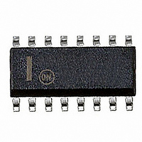
NCP1396BDR2G ON Semiconductor, NCP1396BDR2G Datasheet - Page 15

NCP1396BDR2G
Manufacturer Part Number
NCP1396BDR2G
Description
IC CTRLR OVP HV 16SOIC
Manufacturer
ON Semiconductor
Type
High Performance Resonant Mode Controllersr
Datasheet
1.NCP1396BDR2G.pdf
(25 pages)
Specifications of NCP1396BDR2G
Pwm Type
Voltage Mode
Number Of Outputs
1
Frequency - Max
575kHz
Duty Cycle
52%
Voltage - Supply
10.5 V ~ 20 V
Buck
No
Boost
No
Flyback
No
Inverting
No
Doubler
No
Divider
No
Cuk
No
Isolated
Yes
Operating Temperature
-40°C ~ 125°C
Package / Case
16-SOIC (3.9mm Width, 15 Leads)
Frequency-max
575kHz
Output Voltage Range
20 V
Output Current
300 uA
Power Dissipation
42 mW
Operating Temperature Range
- 40 C to + 125 C
Mounting Style
SMD/SMT
Input Voltage
12V
Frequency
500kHz
Supply Voltage Range
20V
Digital Ic Case Style
SOIC
No. Of Pins
16
Svhc
No SVHC (15-Dec-2010)
Base Number
1396
Rohs Compliant
Yes
Lead Free Status / RoHS Status
Lead free / RoHS Compliant
Other names
NCP1396BDR2GOS
NCP1396BDR2GOS
NCP1396BDR2GOSTR
NCP1396BDR2GOS
NCP1396BDR2GOSTR
Available stocks
Company
Part Number
Manufacturer
Quantity
Price
Company:
Part Number:
NCP1396BDR2G
Manufacturer:
ON Semiconductor
Quantity:
313
converter in case the FB pin cannot rise above 0.6 V (to
actually close the loop) in less than a duration imposed by
the programmable timer. Please refer to the fault section for
detailed operation of this mode.
VCO control voltage will be constrained between 0.5 V
and 2.3 V, whereas the feedback loop will drive pin 6 (FB)
between 1.2 V and 5.3 V. If we take the default FB pin
excursion numbers, 1.2 V = 50 kHz, 5.3 V = 500 kHz, then
the VCO maximum slope will be:
depending on the feedback pin voltage level in a different
frequency clamp combination.
This techniques allows us to detect a fault on the
As shown on Figure 32, the internal dynamics of the
Figures 33 and 34 portray the frequency evolution
Fault
area
Fmax
Fmin
Figure 32. The OPAMP Arrangement Limits the
V
VCO Modulation Signal between 0.5 and 2.3 V
CC
22 kΩ on pin 4 and Rfmax = 1.3 kΩ on pin 2
Figure 33. Maximal Default Excursion, Rt =
F
Mu&Lu
0.6 V
FB
1.2 V
500 k − 50 k
R2
8.7 k
R1
11.3 k
ΔVFB = 4.1 V
100 k
4.1
R3
= 109.7 kHz∕V
D1
2.3 V
5.3 V
No variations
Vref
0.5 V
+
+
- -
ΔFsw = 450 kHz
50 kHz
VFB
500 kHz
Fmax
Rfmax
http://onsemi.com
15
now been reduced to 300 k / 4.1 = 73 kHz / V on Mupper
and Mlower outputs. This offers a mean to magnify the
feedback excursion on systems where the load range does
not generate a wide switching frequency excursion. Thanks
to this option, we will see how it becomes possible to
observe the feedback level and implement skip cycle at
light loads. It is important to note that the frequency
evolution does not have a real linear relationship with the
feedback voltage. This is due to the deadtime presence
which stays constant as the switching period changes.
deadtime) requires the usage of the selection charts
displayed below:
Figure 34. Here a different minimum frequency was
Figure 35. Maximum Switching Frequency Resistor
Please note that the previous small- - signal VCO slope has
The selection of the three setting resistors (Fmax, Fmin
650
550
450
350
250
150
Fault
area
Fmax
50
Fmin
Selection Depending on the Adopted Minimum
programmed as well as a maximum frequency
1.5 3.5
F
Mu&Lu
0.6 V
1.2 V
5.5
Switching Frequency
ΔVFB = 4.1 V
7.5
RFmax (kΩ)
excursion
9.5
11.5 13.5 15.5 17.5
5.3 V
Fmin = 200 kHz
Fmin = 50 kHz
No variations
ΔFsw = 300 kHz
V
FB = 6.5 V
DT = 300 ns
150 kHz
VFB
450 kHz
CC
= 12 V


