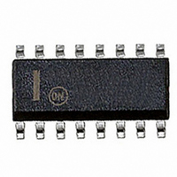
MC33025DWR2G ON Semiconductor, MC33025DWR2G Datasheet - Page 11

MC33025DWR2G
Manufacturer Part Number
MC33025DWR2G
Description
IC CTRLR PWM HS DBL END 16-SOIC
Manufacturer
ON Semiconductor
Datasheet
1.MC34025DWR2G.pdf
(20 pages)
Specifications of MC33025DWR2G
Pwm Type
Voltage/Current Mode
Number Of Outputs
2
Frequency - Max
1MHz
Duty Cycle
45%
Voltage - Supply
10 V ~ 30 V
Buck
No
Boost
No
Flyback
No
Inverting
No
Doubler
No
Divider
No
Cuk
No
Isolated
Yes
Operating Temperature
-40°C ~ 105°C
Package / Case
16-SOIC (0.300", 7.5mm Width)
Frequency-max
1MHz
Duty Cycle (max)
45 %
Output Voltage
5.05 V to 5.15 V
Output Current
500 mA
Mounting Style
SMD/SMT
Switching Frequency
1000 KHz
Operating Supply Voltage
30 V
Maximum Operating Temperature
+ 105 C
Fall Time
30 ns
Minimum Operating Temperature
- 40 C
Rise Time
30 ns
Synchronous Pin
Yes
Topology
Half-Bridge, Push-Pull
Lead Free Status / RoHS Status
Lead free / RoHS Compliant
Available stocks
Company
Part Number
Manufacturer
Quantity
Price
Company:
Part Number:
MC33025DWR2G
Manufacturer:
ON
Quantity:
1 000
Part Number:
MC33025DWR2G
Manufacturer:
ON/安森美
Quantity:
20 000
The addition of an RC filter will eliminate instability caused by the leading edge spike on the current waveform. This sense signal can also
be used at the ramp input pin for current mode control. For ramp compensation it is necessary to know the gain of the current feedback
loop. The gain can be calculated by:
Additional dead time can be added by the addition of a dead
time resistor from V
more information.
Figure 27. Primary Side Current Sensing
R
T
R
Figure 24. Dead Time Addition
DT
V
ref
C
ref
T
to C
4
5
6
9
T
. See text on oscillator section for
The addition of an RC filter will eliminate instability caused by the
leading edge spike on the current waveform. This sense signal
can also be used at the ramp input pin for current mode control.
For ramp compensation it is necessary to know the gain of the
current feedback loop. If a transformer is used, the gain can be
calculated by:
Oscillator
R
w
Figure 26. Resistive Current Sensing
I
Sense
http://onsemi.com
A
A
i
i
+
+
9
turns ratio
turns ratio
11
R Sense
R
w
The sync pulse fed into the clock pin must be at least 3.9 V. R
and C
circuit is also used in voltage mode operation for master/slave
operation. The clock signal would be coming from the master
which is set at the desired operating frequency, while the slave
is set 10% slower.
5.0 V
0 V
T
Figure 25. External Clock Synchronization
need to be set 10% slower than the sync frequency. This
Figure 28. Primary or Secondary Side
R
T
I
Sense
Current Sensing
C
9
T
4
5
6
R
w
Oscillator
I
0
Sense
T


